Baofeng UV-17 Pro GPS handheld radio internals
Older Baofeng radio models often included internal pictures which were available to view in the public FCC filing. However, for recent radio models Baofeng has requested long-term confidentiality for the internal photos (the schematic, block diagram, set-up procedure and operation description were already under long-term confidentiality on previous models).
Of course, since the radio isn’t welded shut, this doesn’t stop anyone from making a detailed investigation of what is in the radio, and that’s what I set out to do.
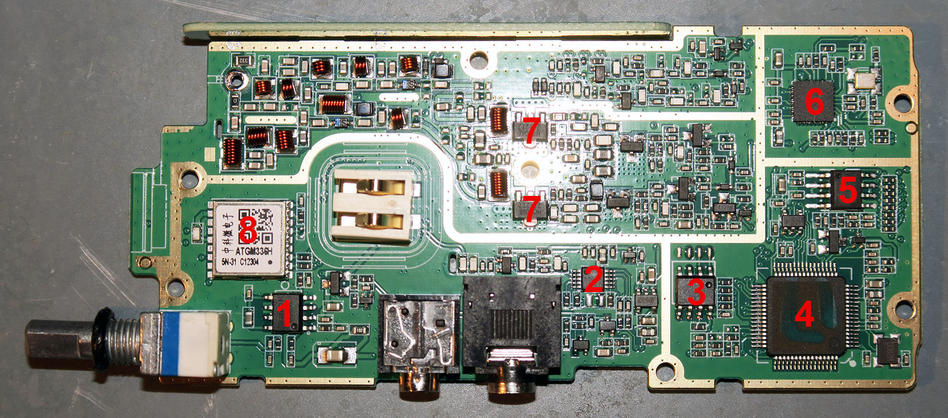
Without further ado, let’s dive right in. This is the side of the radio board that you will see upon initial disassembly (after removal of the LCD display screen):
- LCD display connector – the large solder pad to the left is where the antenna connector is soldered to the PCB
- Front panel (keypad / microphone / speaker / LEDs) connector
- Unidentified integrated circuit from 3PEAK labeled DM2S04B
- GPS antenna connector (UFL) – to the left of the GPS connector are the 2 LEDs that light up the activity indicator at the top of the case.
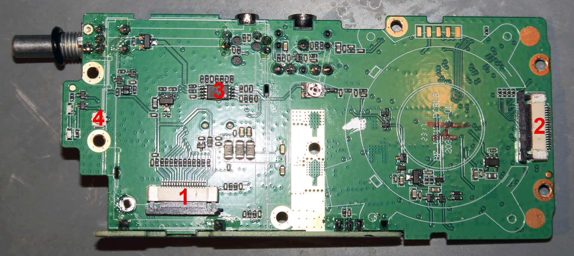
The back side of the board is where things really get interesting (note that you will need to de-solder the antenna connector to get the board out of the chassis):
- TDA2822A – STMicroelectronics dual audio amplifier
- 5807M – RDA Microelectronics FM tuner
- XM25QH16CHIG – XMC 16Mbit serial flash (2MB)
- Microcontroller – Unknown brand/model as the top has been ground off, tentatively identified as an ARM Cortex-A4 family part
- M21529010 – Unknown IC, possibly flash memory
- FD6818 – RF transceiver
- H0606E – RF power transistors
- ATGM336H-5N – Zhongke Microelectronics GPS / Baidu receiver
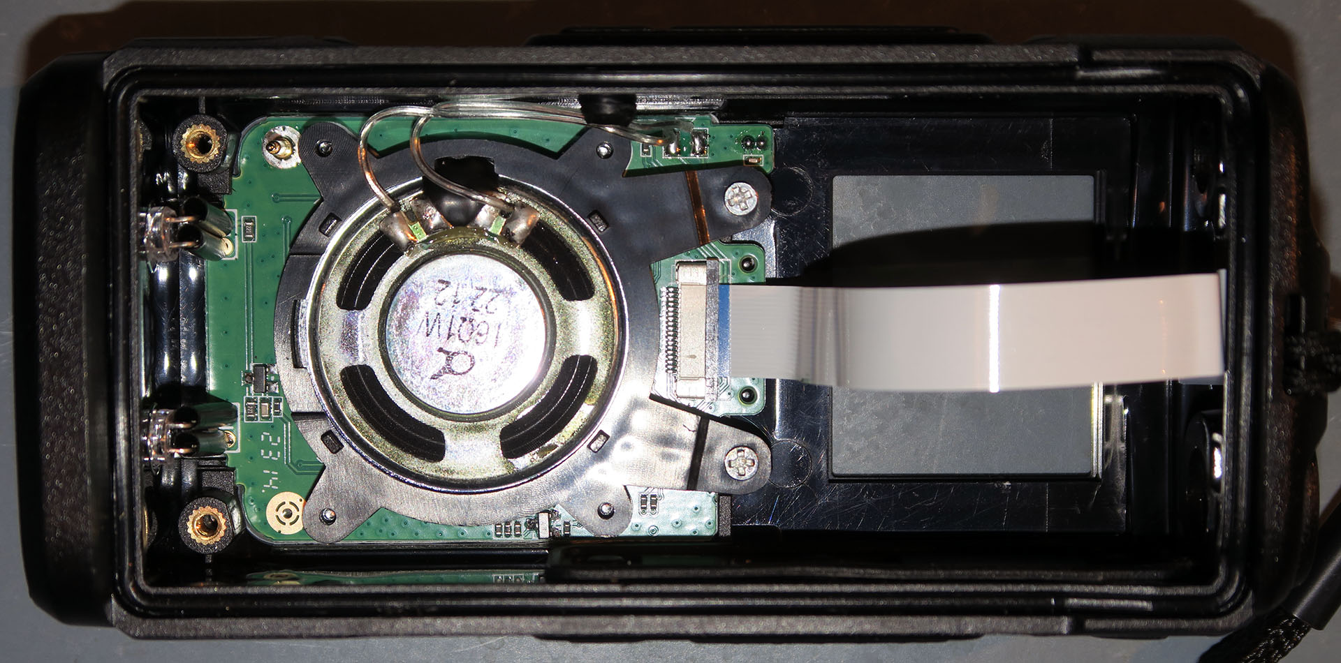
This is the underside of the front panel (keypad / microphone / speaker / LEDs). I did not do further disassembly in this area. But the LEDs and their driver transistor are visible at the left of this image. The PCB artwork is dated 2314, so is apparently quite recent.
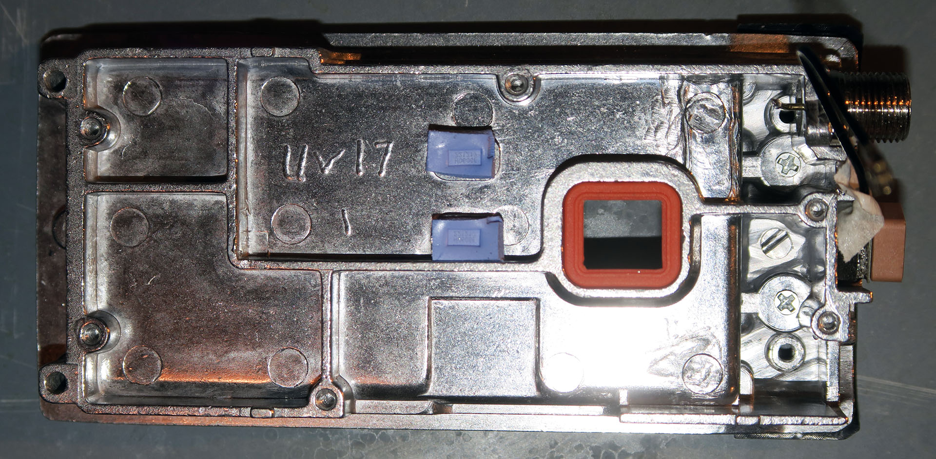
This is the baseplate, which doubles as a heat sink for the 2 RF output transistors (the blue pads). The coarse scrawl of “UV-17 1” is quite different than the care shown in the rest of the radio internals:
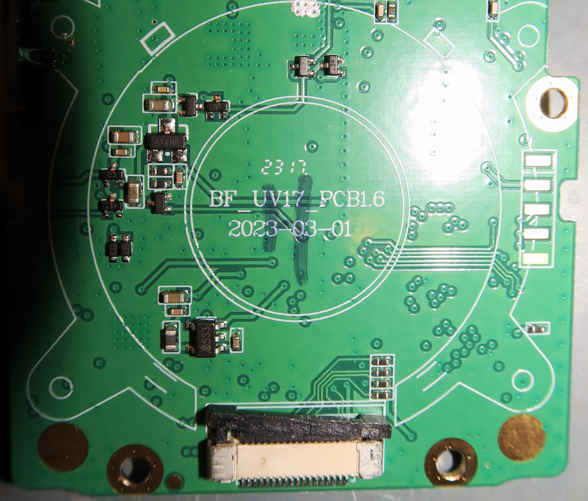
This closeup shows the identification markings on the main PCB – “BF_UV17_PCB1.6 / 2023-03-01” with PCB artwork dated 2317. The row of 5 fingers at the center right is connected to the CPU, possibly used for programming the firmware:
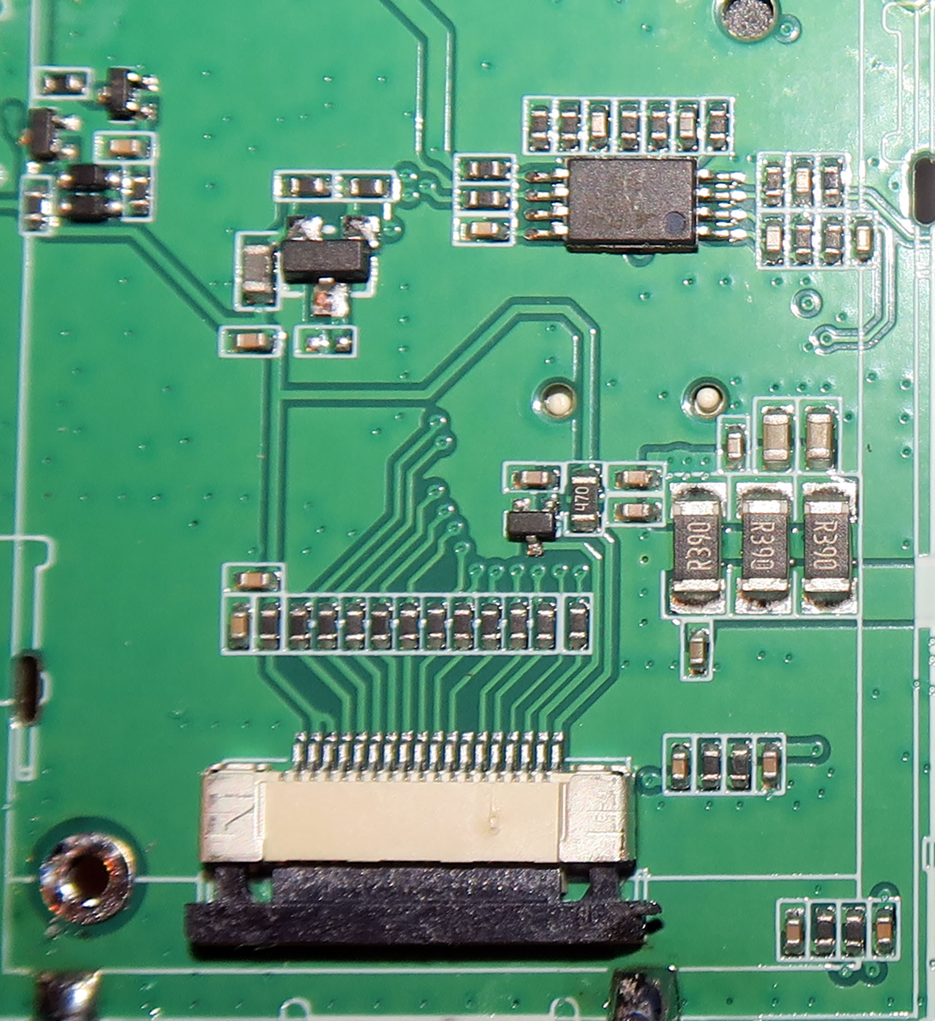
In contrast to pictures posted of older model radio internals, the wave soldering seems to be quite well-done on this board:
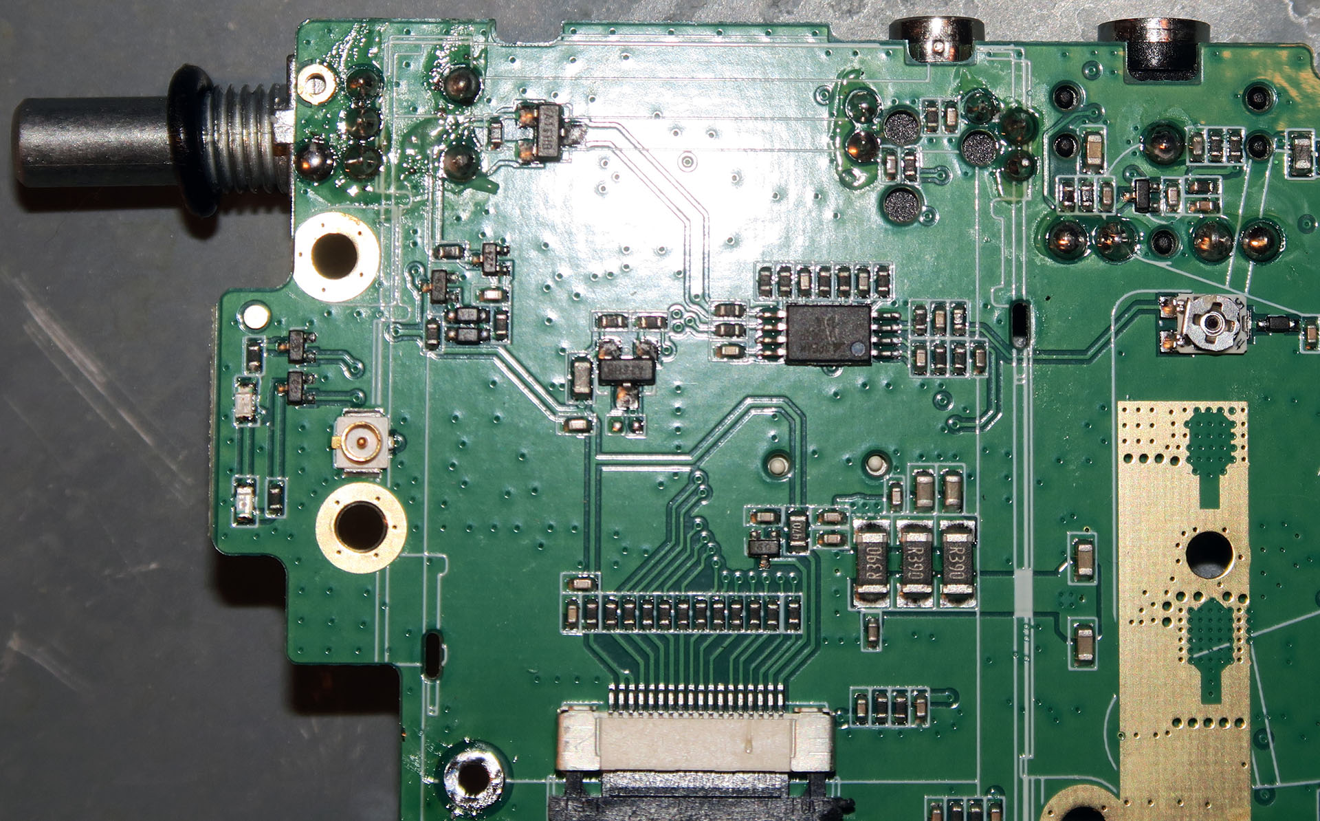
In this picture you can see the hand-soldering of items like the volume control and the K1 external microphone / speaker connector:
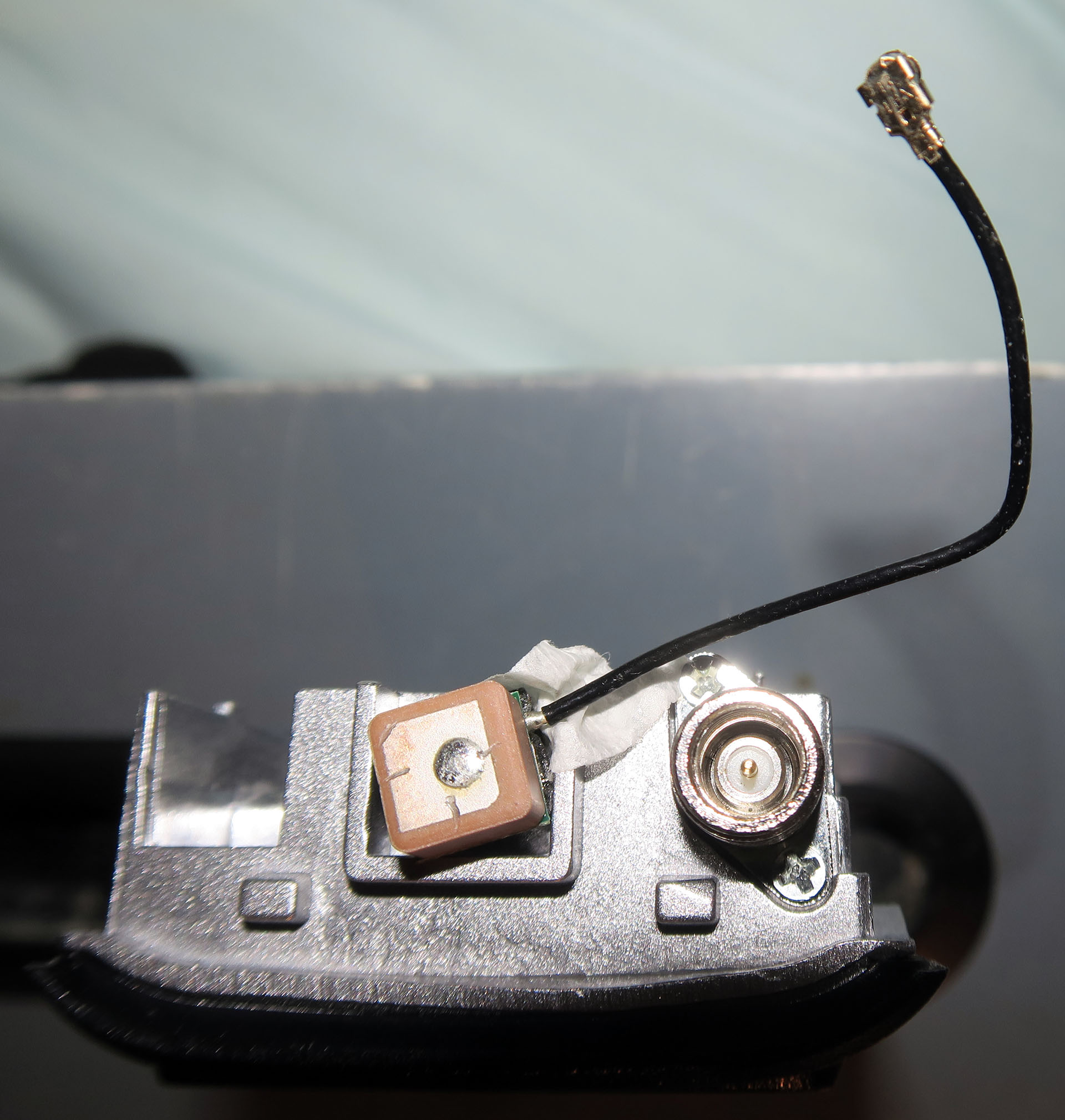
I’ll wrap up this post with a picture of the GPS patch antenna. It is a “dumb” antenna – all of the magic happens in the ATGM336H-5N chip: