Archive for the 'Computer History' Category

Senator Ted Stevens’ Internet envisioned as a series of tubes

15 years ago, on June 28th 2006, Alaska’s Senator Ted Stevens said that “… the Internet is … a series of tubes”. While widely ridiculed at the time for failing to understand the nature of the services his Senate committee was in charge of regulating, I figured I’d take a look back on the occasion of the quote’s 15th anniversary. The following text is intended as humor – please don’t tell me that I don’t “get it” either.

While the Internet is indeed “a series of tubes”, very few people have actually seen these tubes and generally think (if they think about them at all) that they are as mythical as unicorns. In reality, the tubes are quite shy and generally burrow deep underground, where they are neither seen nor heard as they happily carry the Internet traffic of billions of users. Despite being solitary by nature, sometimes the tubes are forced by humans into larger groups for ease of herding. Even in captivity, the tubes do reproduce by fission, generally as one or more new, thinner tubes branching off of the parent tube. An example can be seen in the rectangular box near the foreground of the image.

As I mentioned, the tubes are generally solitary and out of sight, so most people don’t know what they look like. So I am pleased to show you this image of a large group of tubes at one of the main places humans have forced them together. This may be the only time people will ever see such a large gathering of tubes.


This image is clickable for a larger view

This image was taken in October, 2019 at 111 Eighth Avenue, NYC (AKA the Googleplex), although this photo was taken in a public corridor. The exact location is the 5th floor near the 9th Avenue end of the building. And yes, I really did take this picture nearly two years ago with the specific intent of making this post today.

This specific post and image are licensed under the Creative Commons Attribution-NonCommercial-ShareAlike 4.0 International (CC BY-NC-SA 4.0) license. Contact the author here if you would like to discuss alternative licensing and usage.

The Datatran Datatracker DT-5 RS-232 Breakout Box

If you’ve come here just looking for the Datatracker DT-5 manual, you can download it here if you want to skip the long walk down Memory Lane.

A little history

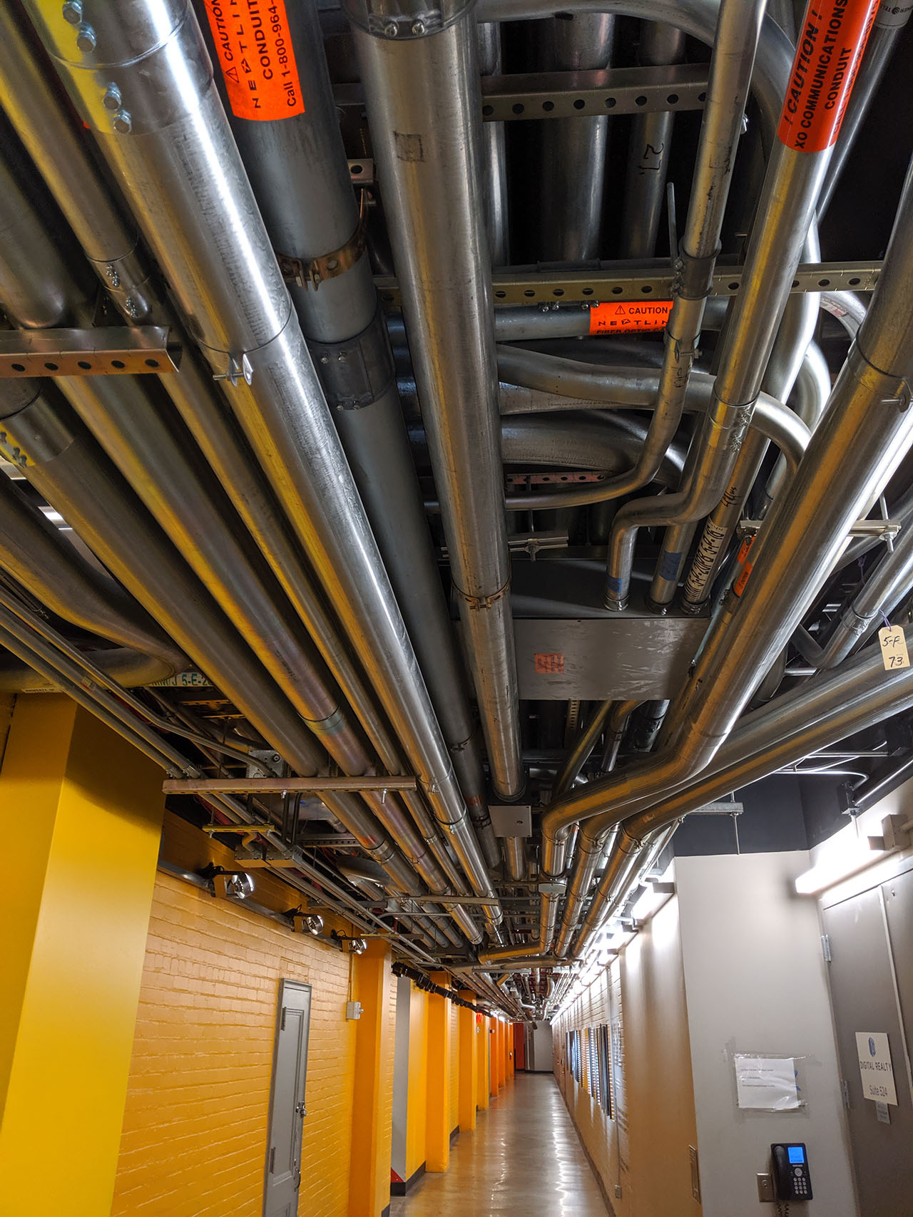
Long before there was Ethernet, computers were connected to terminals, modems, etc. via a huge number of different possible cabling systems. Even earlier on, mechanical teleprinters were connected to switching systems such as TELEX and TWX. One of the most popular connection types, particularly in later years as 20mA type connections were phased out, was called “RS-232”. The “RS” in there stands for “Recommended Standard” – in other words, “Wouldn’t it be a wonderful world if everything worked this way?” dreaming. The original version of this standard was published in May, 1960 and the most popular version, RS-232-C, was published in August, 1969. RS-232-D was published in 1986, RS-232-E in 1991 and RS-232-F in 1997. To be honest, I’d never heard of the -E or -F revisions until I was doing research for this article.

Wikipedia describes it thusly: “Because the standard did not foresee the requirements of devices such as computers, printers, test instruments, POS terminals, and so on, designers implementing an RS-232 compatible interface on their equipment often interpreted the standard idiosyncratically. The resulting common problems were non-standard pin assignment of circuits on connectors, and incorrect or missing control signals. The lack of adherence to the standards produced a thriving industry of breakout boxes, patch boxes, test equipment, books, and other aids for the connection of disparate equipment. A common deviation from the standard was to drive the signals at a reduced voltage. Some manufacturers therefore built transmitters that supplied +5V and −5V and labeled them as ‘RS-232 compatible’.” In other words, it was pretty much the Wild West out there.

Note that I disagree with one aspect of the Wikipedia article – +/-5V is a perfectly valid signalling level for RS-232-C as the standard specifies minimum voltages of +/-3V to +/-15V. In practice, “classic” RS-232 drivers normally operated from +/-12V as those were common power supply voltages in older computers. The incredibly popular MAX232 series (datasheet PDF) generates RS-232 levels of between +/-5V and +/-8V and I’ve never heard of interoperability issues with those parts.

Being the Wild West, there was a need for hired gunslingers to sort out problematic cabling. I was one of those gunslingers – for example, in the mid 1980’s a major New York bank flew me first class from the US to Venezuela (I have some interesting stories about Venezuela, but I’ll save those for another time) and set me up in a hotel suite for a week, just to install a bisync protocol converter on their IBM 4381 mainframe. And yes, they paid for my flight home, too!

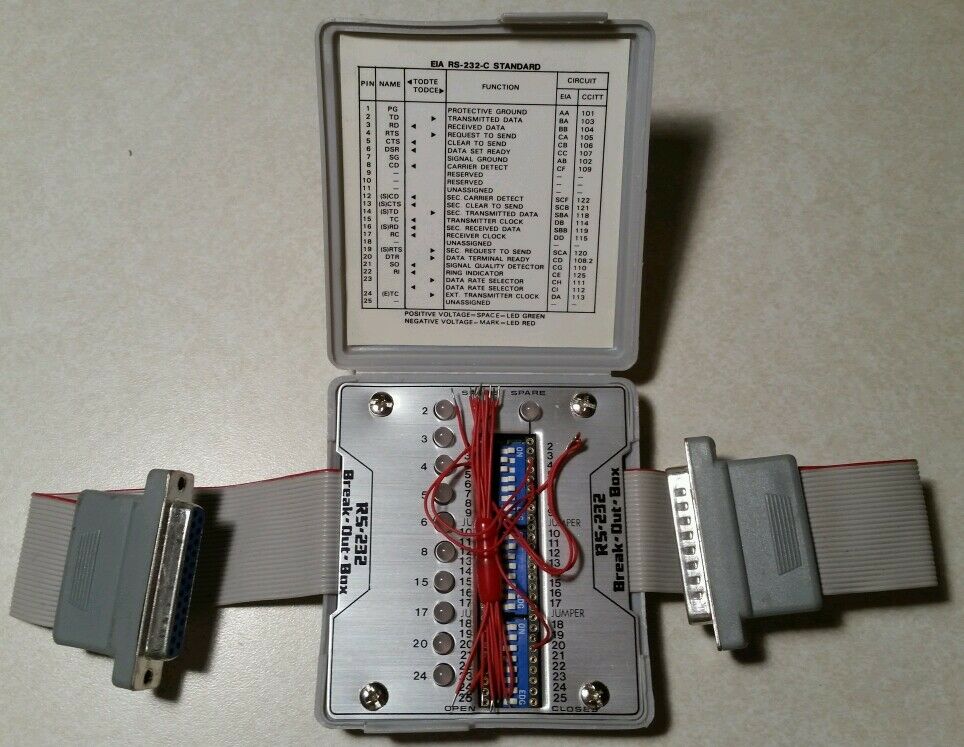
The average breakout box of that era had a few LEDs to indicate signals and jumper wires to manually patch signals from one side of the box to the other. This TENMA 72-440 is a typical breakout box:


This and all subsequent images are clickable for a larger view

Enter the Datatracker

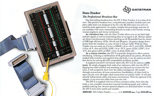
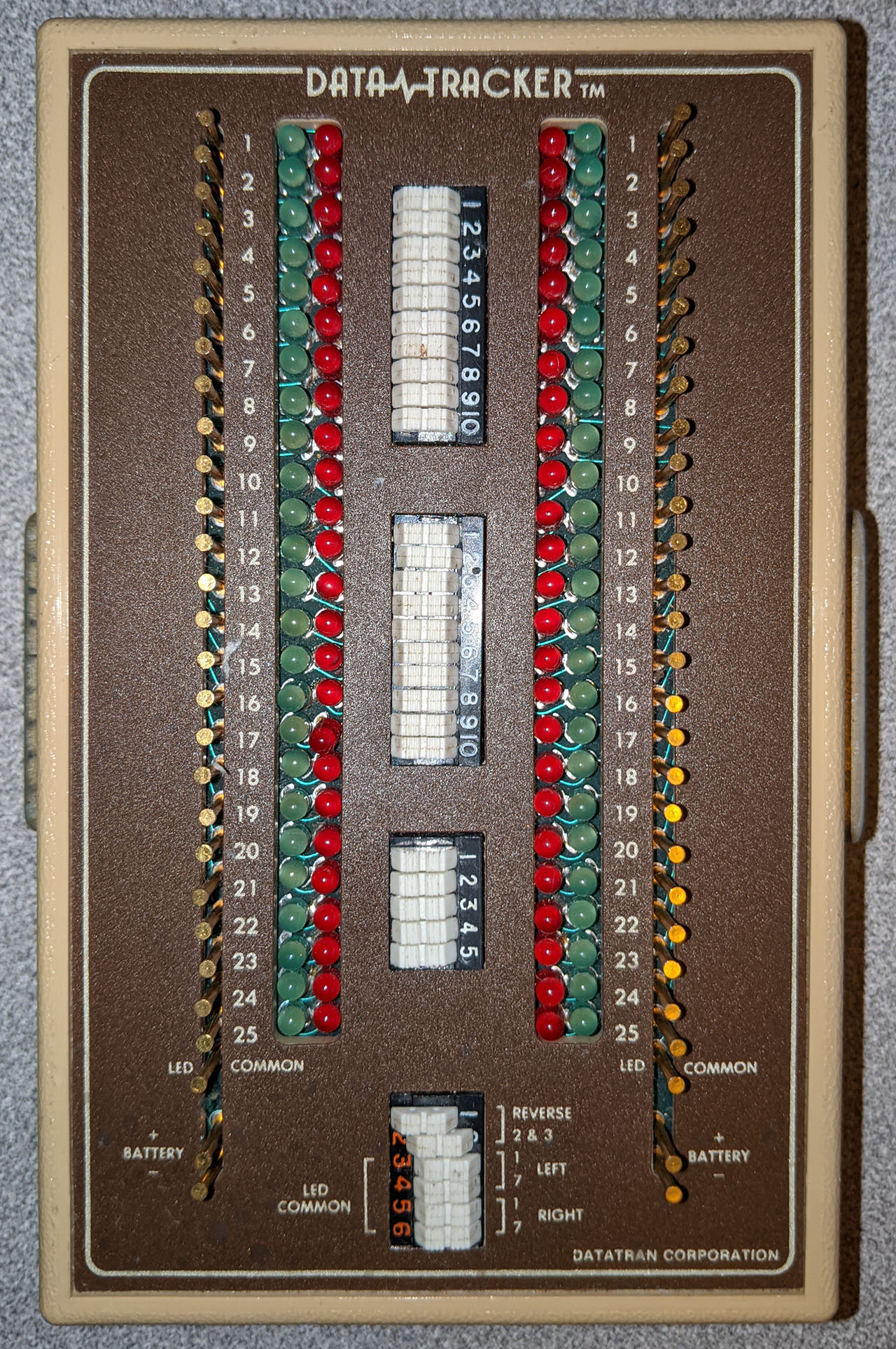
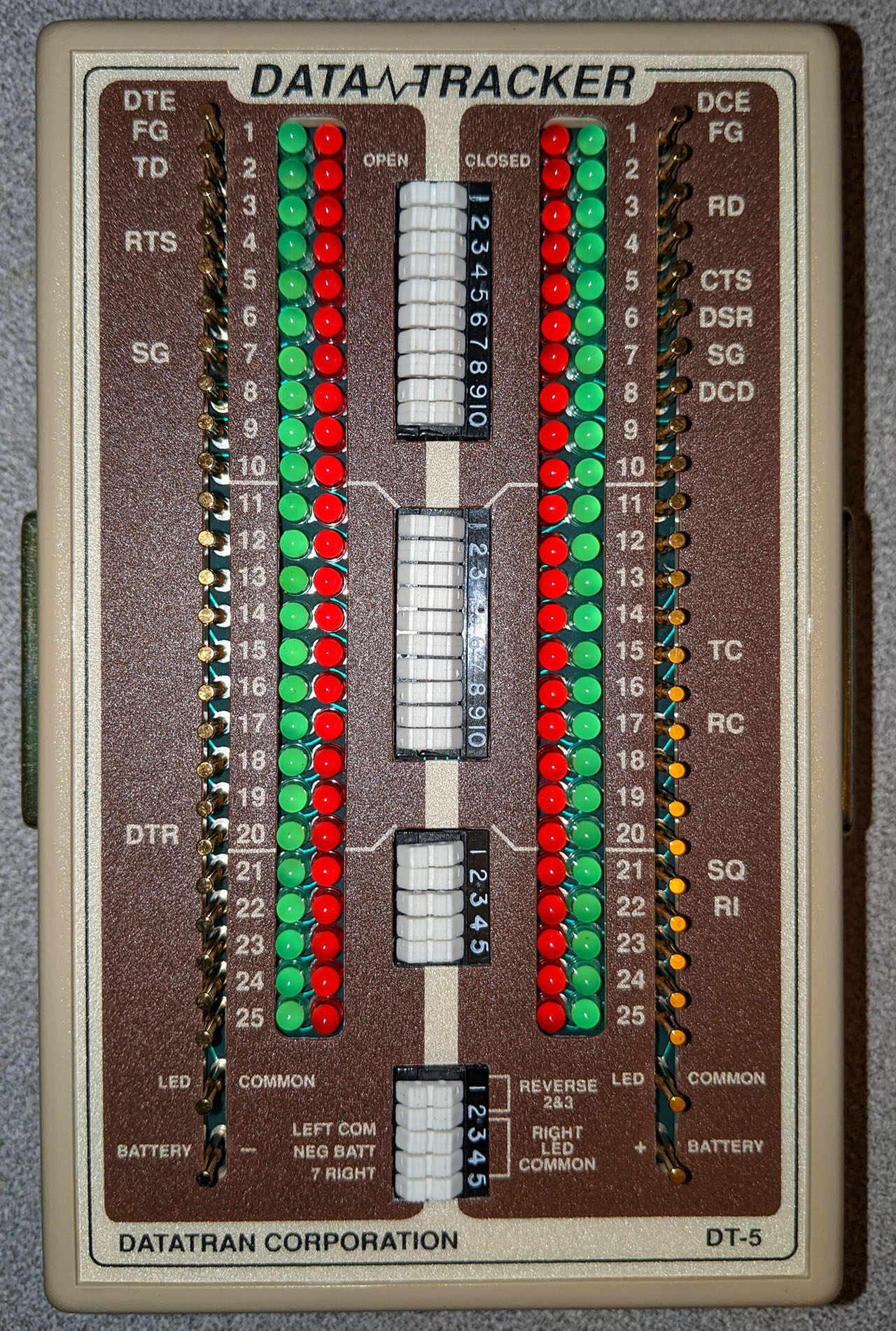
That type of breakout box is fine if you’re solving minor incompatibilities, but if you’re in a foreign country 2000+ miles away from home, you want the most complete breakout box possible. In my case, that was the Datatracker DT from Datatran Corporation. This was a box with 100 (!) LEDs, displaying a high / low signal for each of the 25 pins on each side of the breakout box, as well as being able to supply positive and negative voltages to force any pin on either side to a specific state.

This is the product listing from the Specialized Products Fall ’95 product catalog, showing the final iteration of the Datatracker, the DT-5. Note that $239 in 1995 dollars is over $400 today:

As I mentioned, there have been several iterations of the Datatracker, with the DT-5 being the final one.

The Datatracker DT-3

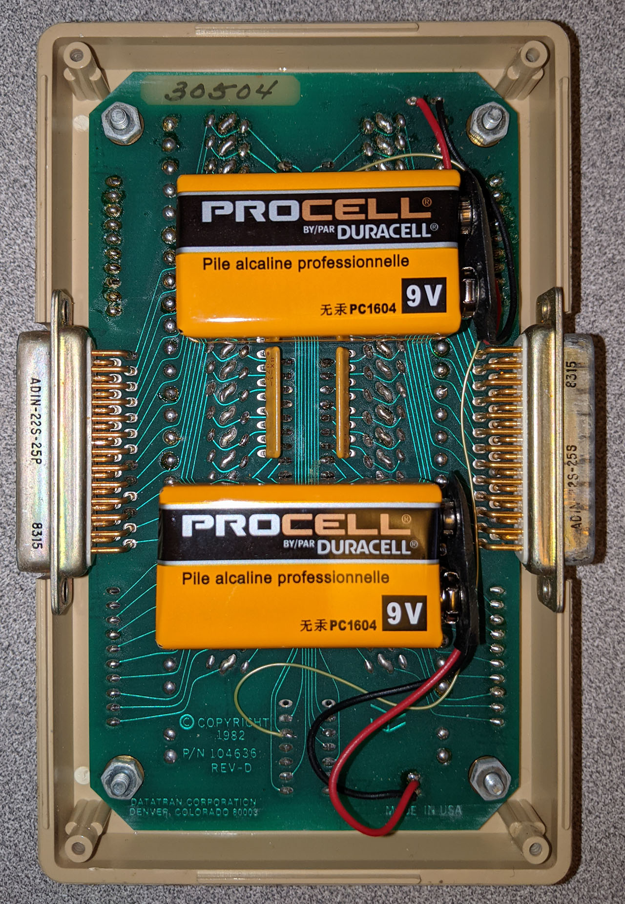
This is my first Datatracker, purchased around 1984. It has a 104636 Rev. D circuit board, copyright 1982. The distinguishing features of this unit are:

  • No external battery access – the case must be opened to access the batteries.
  • Dual batteries, one for providing +V (logic 0) and another for providing -V (logic 1) signal levels.
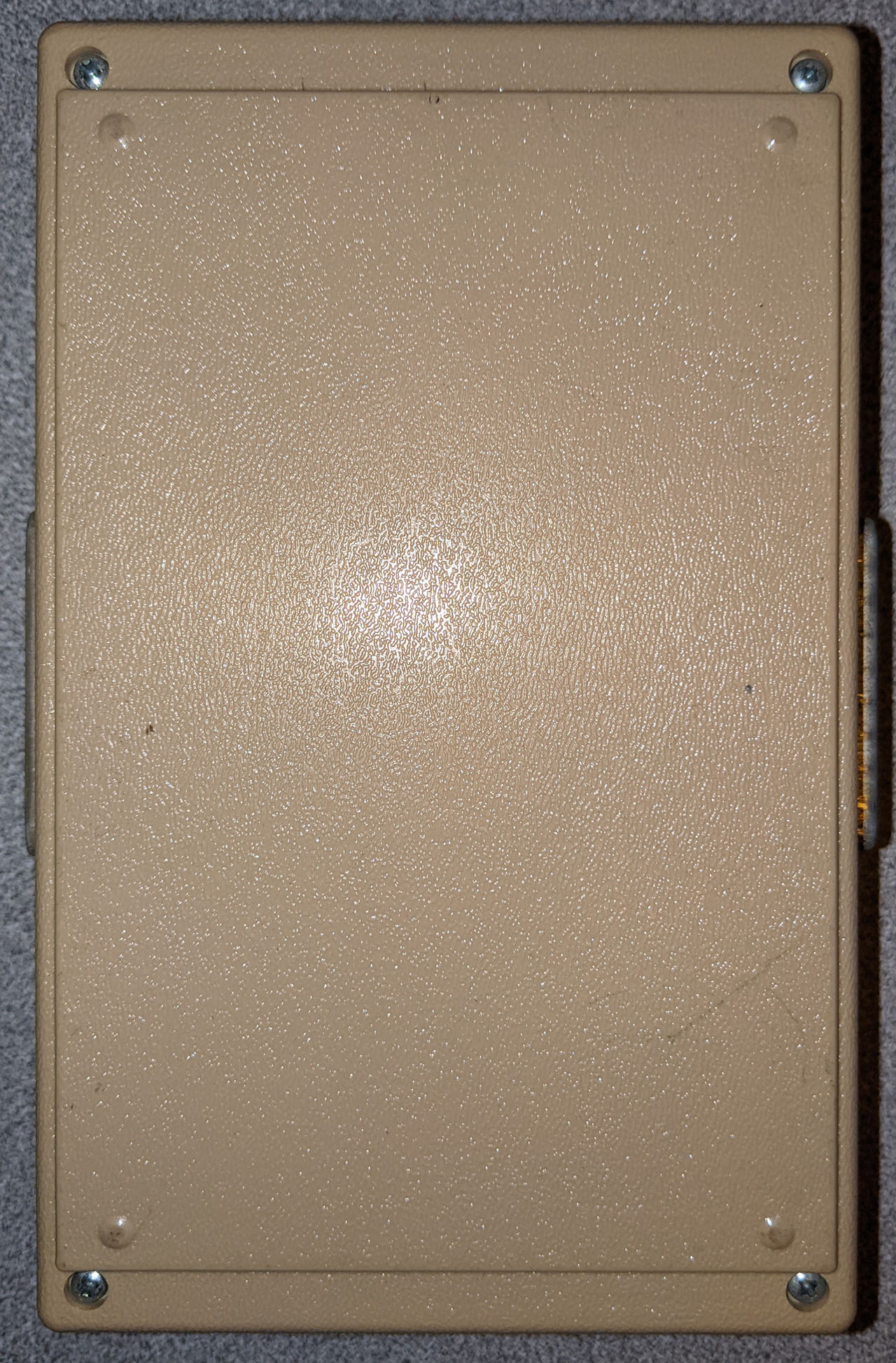
  • No snap-on protective cover and no markings on the outside back of the case
  • The carrying case is long and skinny and contains 4 clip leads and a M/F ribbon cable. One side of the case interior is rubberized to prevent damage to the case from the test pins.
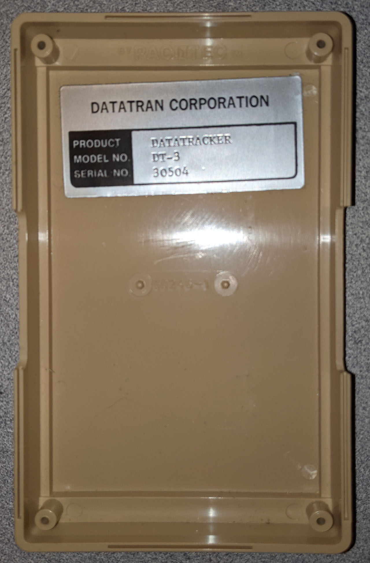
  • Identified on the internal serial number sticker as a model DT-3

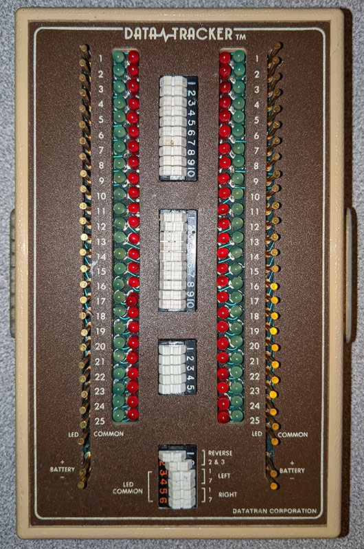
In the above picture you can see that both the left and right battery connections have both a + and a – pin, and there are 4 switches for LED Common – left battery to DB-25 pins 1 and/or 7 and right battery to DB-25 pins 1 and/or 7. To me, this is a major advantage of this version of the Datatracker over the subseqent DT-4 and DT-5 variants. It is possible to generate both a high and a low signal at the same time with this version, a feature that was lost in newer models. It is rare to need both + and – levels and not be able to “borrow” one from another RS-232 signal in the cable, but when you need it, you really need it.

The DT-3 has a plain back cover, lacking both battery access and a listing of common RS-232 signals.

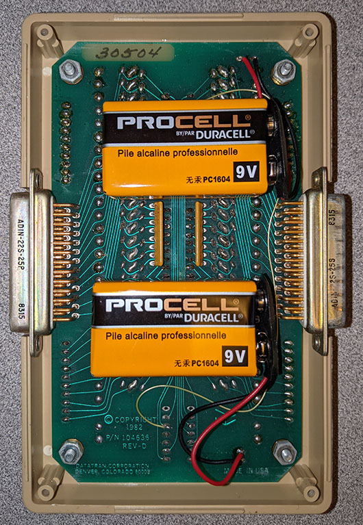
The skinny pale yellow wire wrap wire you can see in the above picture is a repair done by me – the batteries are held in place with double-sided foam tape, and I was overly aggressive when prying the lower battery free to replace it in the mid 1980’s. I damaged one of the printed circuit board traces and repaired it with some wire I had on hand, taking care to route it away from the batteries so it wouldn’t be pulled free during a future battery replacement.

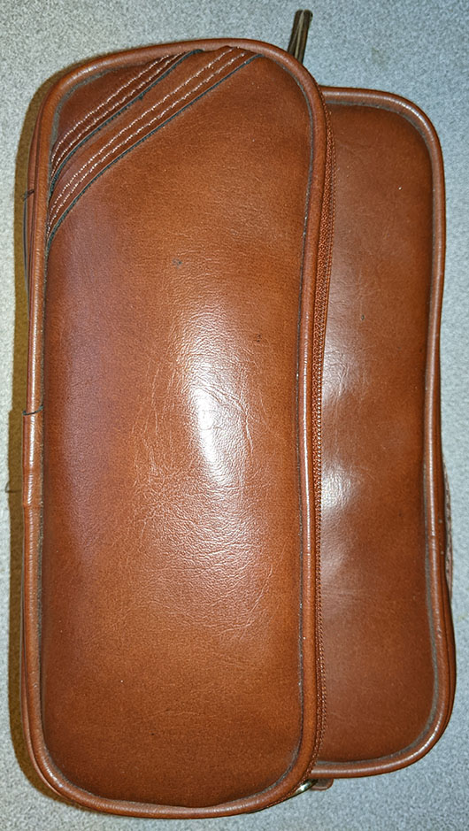
This carrying case holds the Datatracker in the main compartment and the clip leads and DB-25 M/F ribbon cable in the smaller compartment.

Despite the faceplate of this Datatracker being labeled “Datatracker” with no version, we see from this sticker that it is indeed a DT-3 model. By 1984 Datatran had apparently produced over 30,000 of these units.

The Datatracker DT-4 (labeled as a DT-5)

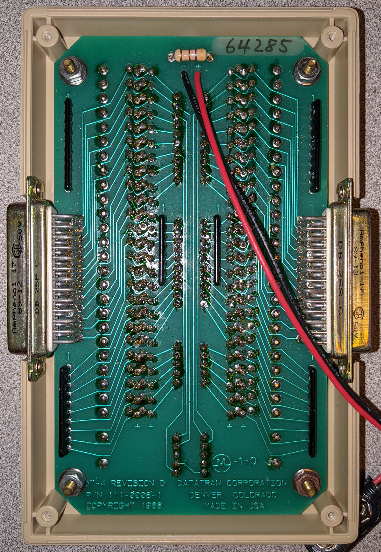
This next Datatracker is a bit of an oddity – The front panel says DT-5 but the circuit board is 111-0008-1 Rev. D and is clearly labeled DT-4, copyright 1988. Compared to the DT-3 above, this unit has:

  • Single externally-accessible battery compartment.
  • Snap-on protective cover for the front of the unit to protect the pins and carrying case.
  • The carrying case is shorter and wider.
  • The LEDs are slightly larger than the ones on the DT-3. I believe they are also somewhat brighter at a given signal level than the ones on the DT-3.
  • A current-limiting resistor was added in the battery circuit to protect against user-configured short circuits.
  • In addition to the 4 clip leads, a ribbon cable with a DB-25M connector at one end and both DB-25 M and F connectors at the other end and a second ribbon cable with a DB-25F connector at one end and both DB-25 M and F connectors at the other are provided.
  • The lower switch assembly is now 5-position instead of 6-position, reflecting the single battery.
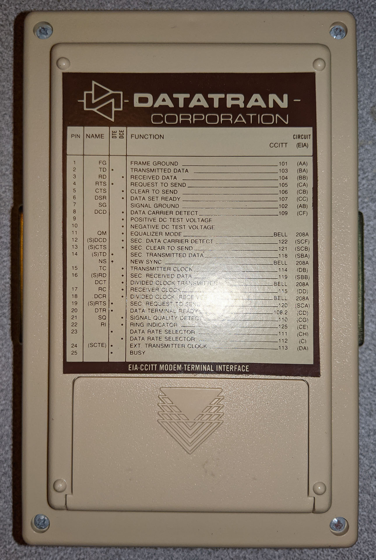
  • Some of the more common pin uses are labeled on the faceplate.

You can see the “DT-5” on the lower right of the faceplate. The LED’s aren’t really all lit – it is just the way they responded to the camera flash.

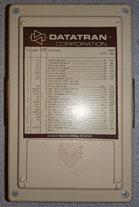
The back panel now has a list of common RS-232 signals and an access panel for replacing the (single) battery.

Despite what the faceplate says, the printed circuit board is clearly labeled “DT-4”. The single resistor directly above where the battery wires connect to the printed circuit board is to provide current limiting if the user accidentally jumpers the battery terminals together.

This shows that this particular unit was manufactured in the eighth week of 1989, and a total of over 64,000 units have been produced to date.

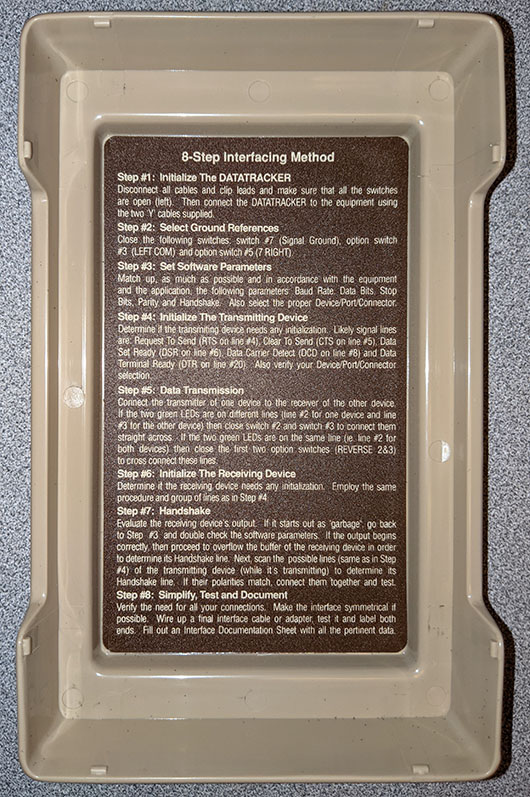
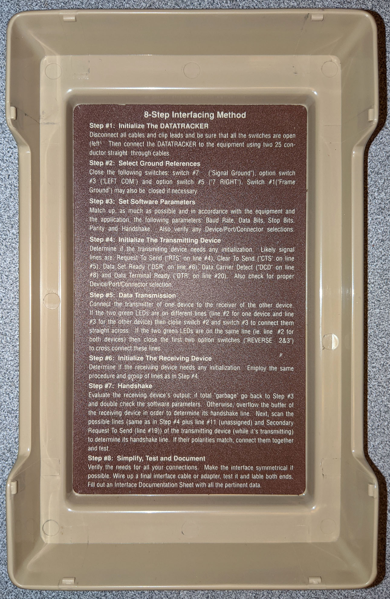
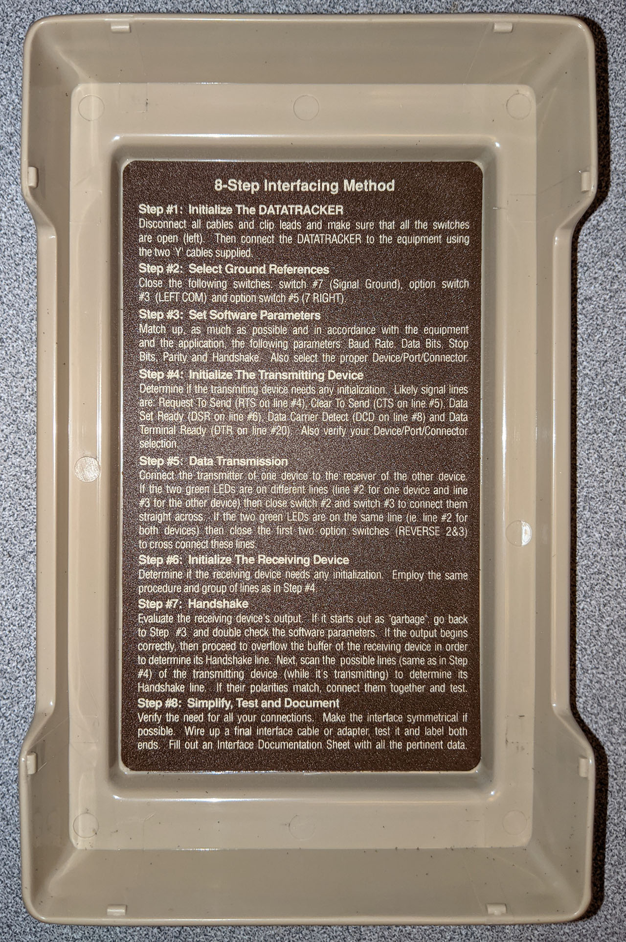
The inside of the snap-on protective cover contains an abbreviated version of the “8-Step Interfacing Method” from the manual. In the manual, it is the entirety of Chapter 4 (20 pages, beginning on page 43 of the PDF linked at the top of this post). Note the typo of “lable” instead of “label” near the bottom.

The Datatracker DT-5

The last Datatracker in this article is labeled DT-5 both on the case and the printed circuit board, which is 111-0049 Rev. A, copyright 1990. In most aspects it is identical to the DT-4. It comes with the same accessories (carrying case, 4 clip leads and two 3-connector DB-25 ribbon cables).

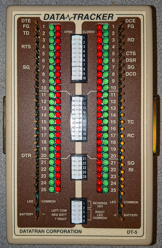
The only externally-visible difference is that the DIP switches are now labeled 1 through 25 instead of two sets of 1 through 10 and the one set of 1 to 5. That’s a nice touch, but hardly a major change.

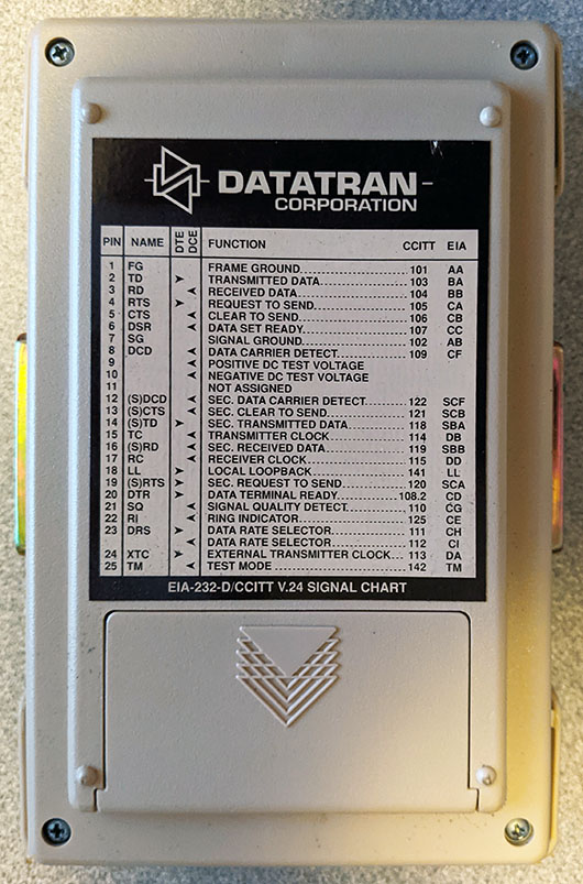
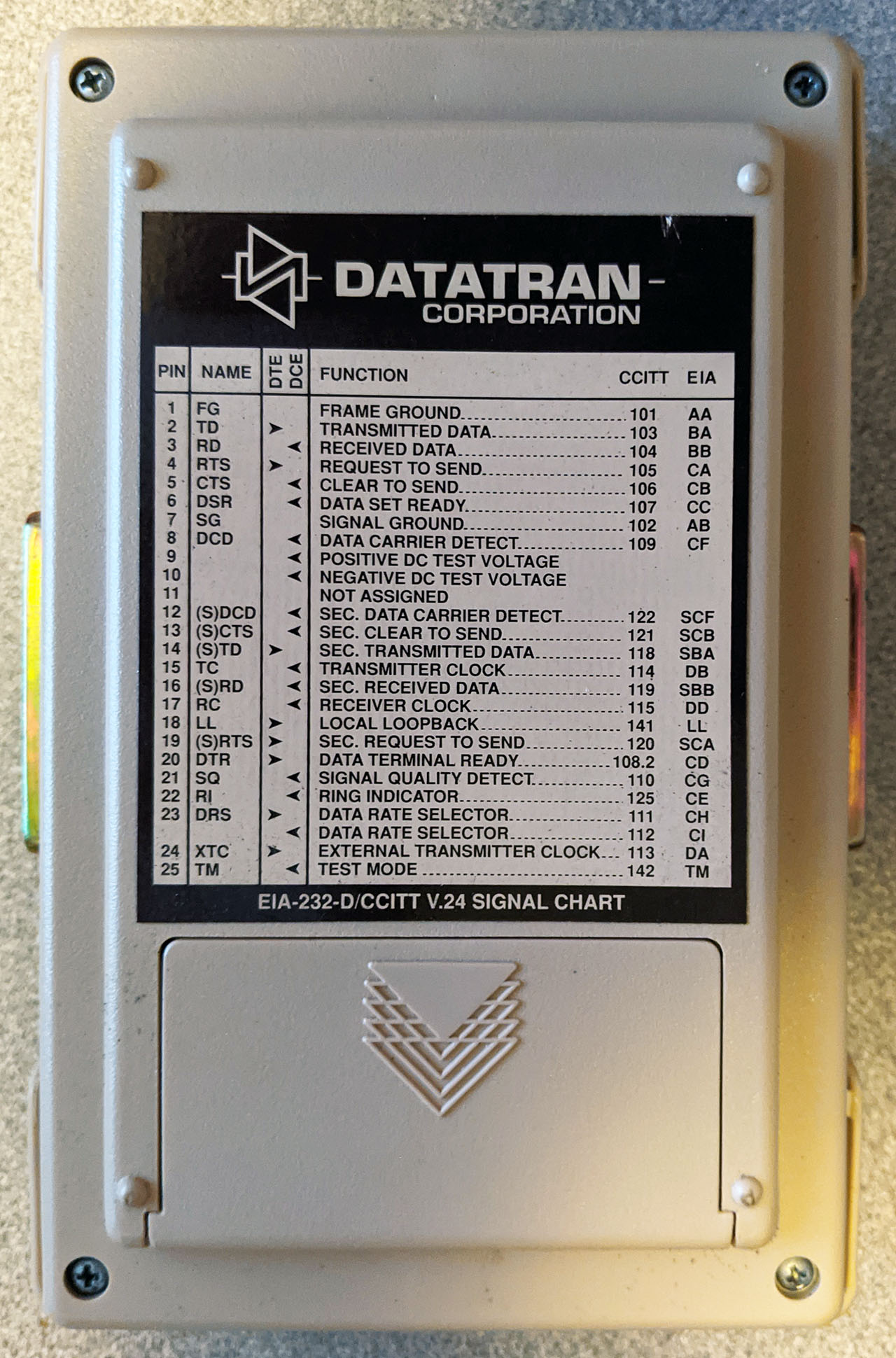
The back panel has a similar list of common signals as the DT-4. However, references to the Bell 208A modem have been removed and the title is now “EIA-232-D/CCITT V.24 SIGNAL CHART”, showing the exact standard numbers and reflecting the changed standard from RS-232-C to RS-232-D.

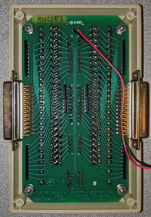
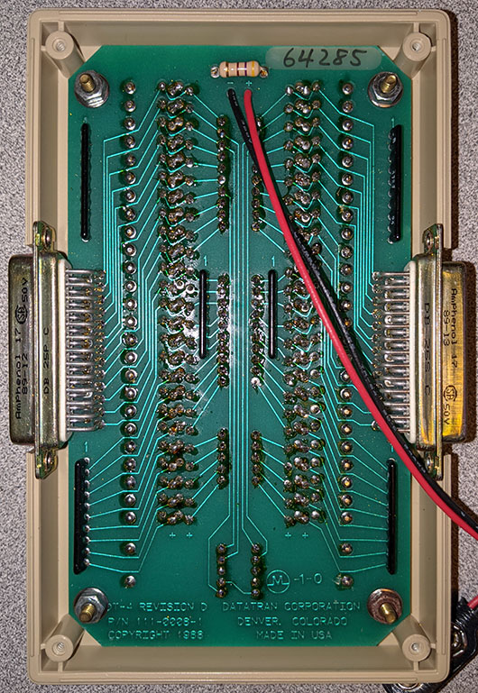
The internal construction appears nearly identical to the DT-4, except that the battery leads have been threaded through the right-hand DB-25 pins, presumably to keep the wires in place when the case is assembled.

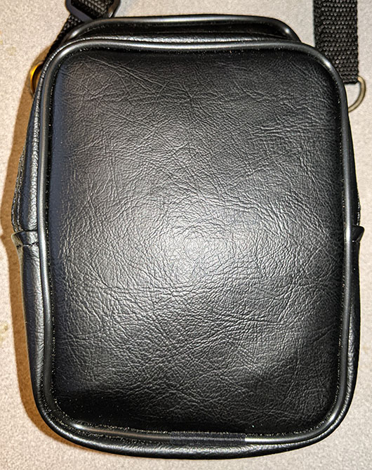
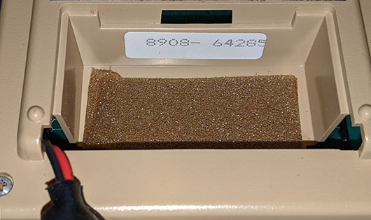
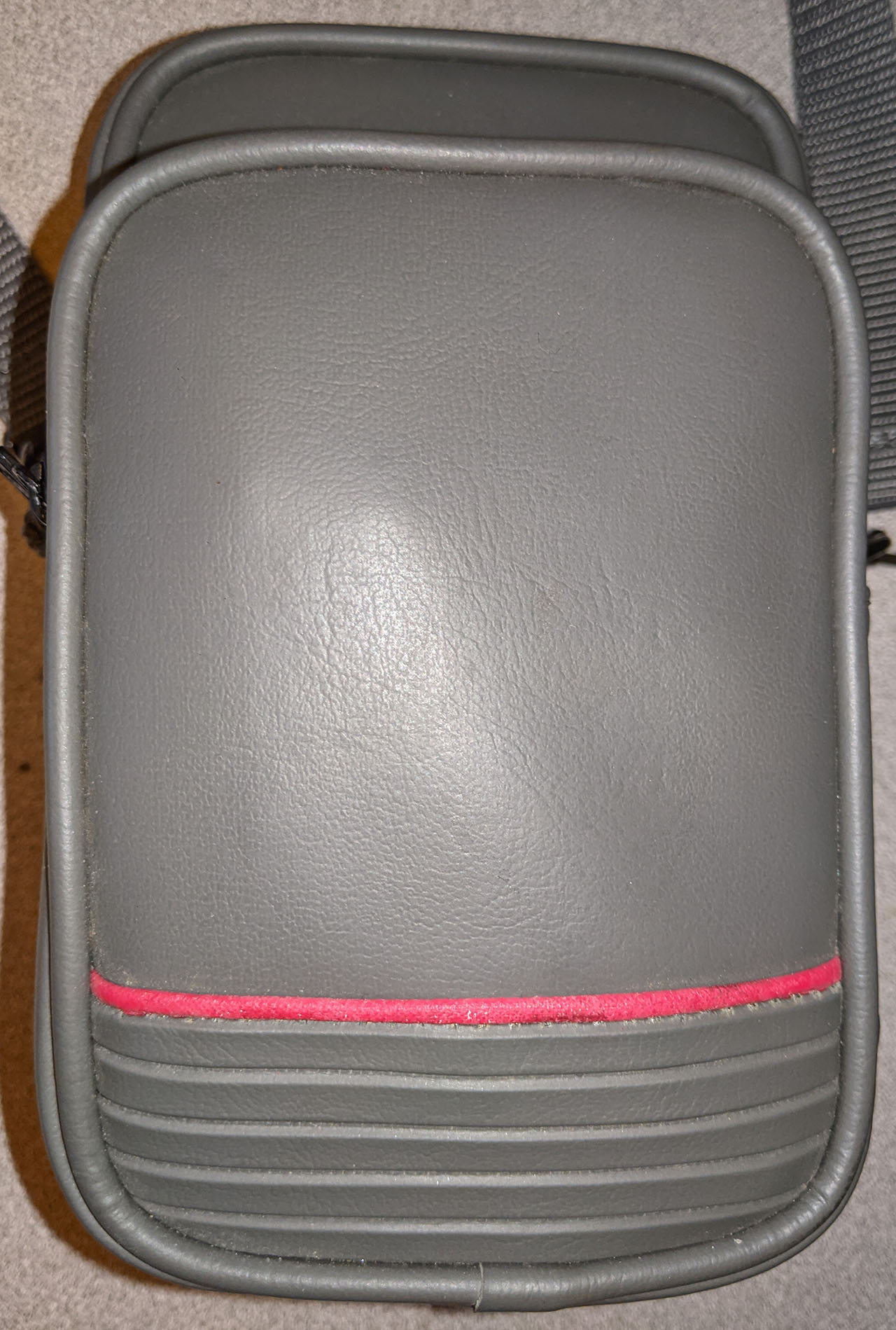
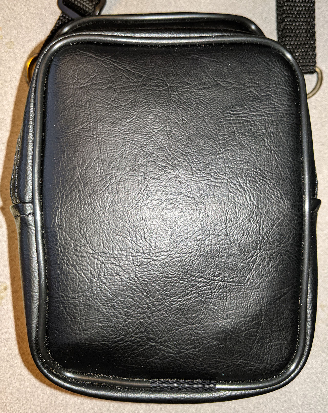
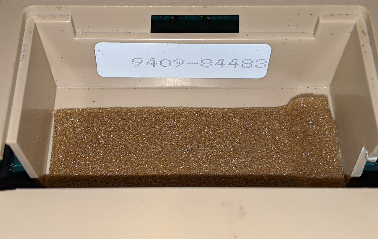
This unit came in a black leatherette carrying case. While a bit more subdued than the case the DT-4 arrived in, the foam inside it has degraded and covered everything with a thin layer of sticky dark grey dust. You can see some of this inside the battery compartment in the next picture.

This unit was manufactured in the 9th week of 1994, with over 84,000 units produced so far. This is likely the last version produced, as the product is not listed in Specialized Equipment catalogs after the Fall ’95 edition.

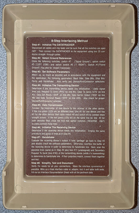
The snap-on cover contains the similar text as the cover for the DT-4. The “lable” typo has been fixed and there are other minor changes such as saying the test cables are “Y” cables.

Conclusion

I hope you’ve enjoyed this walk down Memory Lane. While newer interfaces such as USB and Ethernet have replaced RS-232 in the majority of uses, some commonly used devices such as Cisco routers and switches still have an RS-232 console interface. Every now and then I need to break out one of my Datatrackers to solve a thorny interface problem. The DT-3 is still my preferred device, 35+ years on. I definitely got my money’s worth out of it.

Used Datatrackers for sale can be found on eBay from time to time. As of the time this article was written, the least expensive one is listed for $19.98 and the most expensive one is listed for $65.00. Despite these often being sold “as is”, they are pretty indestructible aside from physical damage. In theory it is possible to damage the LEDs with an overvoltage condition, but that is very rare. The assorted accessories are easily replaced for the most part if they are missing, although you should make sure the unit you’re considering buying has the snap-on cover to protect the unit when not in use. It is very uncommon to find one of these units complete with manual, which is why I have scanned the DT-5 manual and uploaded it here. Also, bitsavers.org is also hosting a reduced-resolution copy of the manual here.

Soviet PDP-11 Clones

In addition to having a domestic computer design industry (see Pioneers of Soviet Computing [local copy]), the Soviet Union was well-known for copying computer designs from the West. While there were many possible reasons for this, one of the most commonly given ones was the desire to run specific software, also from the West. This could be a particular application program or a whole operating system. Certainly, not having to write software in order to have a deliverable computing product was a huge benefit to the Soviets. While the scale of this cloning program was not entirely understood by the West during the Soviet era (see Total Soviet Computing Power [local copy]) it was well known that a good deal of cloning was going on.

Steal the best
Image courtesy of FSU’s Silicon Zoo

DEC supposedly inscribed the phrase “VAX – When you care enough to steal the very best” on an otherwise-unused area of the die for one of their MicroVAX CPUs. The phrase in the picture reads “СВАКС… Когда вы забатите довольно воровать настоящий лучший” which is horribly mangled Russian, but I think it got the point across.


The highest-performing PDP-11 CPU DEC built was based on the DCJ11 (or J-11, or Jaws), microprocessor. This CPU was the basis for all subsequent DEC PDP-11 products (PDP-11/53, /73, /83, /84, /93 and /94) up until they sold the product line to Mentec, who continued to use the J-11 on their M70 / M71 / M80 / M90 and M100 CPUs. It was not until nearly 4 years had elapsed after Mentec acquired the DEC PDP-11 line that they introduced a new design, the M11, not based on the J-11. This was probably due to the last J-11 chips being manufactured in early 1998, as production was apparently stopped as soon as Compaq acquired DEC.

The J-11 design was not without its problems. It was a joint manufacturing effort of DEC and Harris Semiconductor (Intersil). DEC had previously used the Harris / Intersil 61×0 chips, which implemented the PDP-8 CPU in a microprocessor. They probably weren’t expecting the issues which plagued the J-11 project. In addition to problems with the CPU itself, there were problems with the optional floating-point accelerator chip (designed and built entirely by DEC) and the support chips needed to make the J-11 function in a system. This led to a number of costly recalls by DEC to fix (or conceal) problems. The original distinction between the various PDP-11 systems based on the J-11 was lost as parts (normally the floating-point accelerator chip) were removed and / or the board swapped for a slower 15MHz one in the field to get the systems working reliably. Eventually the J-11 systems became reliable enough that users could have an 18MHz CPU with working floating point. Earlier J-11 chips had speed restrictions (often 15MHz) and did not work with the floating-point chip. The planned optional Commercial Instruction Set (CIS) option was never produced, although you can see where it would have been placed on the bottom side of the CPU.

Certainly not all of the problems were on the Harris side – I’ve successfully run a J-11 at 24MHz on a 3rd-party board. The DEC support chip set was found to be limited to a bit over 18 MHz, which is why DEC did not press Harris particularly hard to meet the 20MHz design goal (for top-binned parts). The part number DCJ11-AE (the -AE suffix indicated the revision level) was the last version produced, the “good one”. Interestingly, the individual chips on the first DCJ11-AE CPUs were revision 1 on the DC334 chip and revision 11 on the DC335. The newest DCJ11-AE I’ve seen (with a module date code of 9820 and chip date codes of 9819) has a revision 4 DC334 chip and a revision 16 DC335 chip. That DCJ11-AE has the Harris logo stamped on the ceramic carrier as well as the individual chips, while a somewhat earlier sample with a 9711 date code has the same revision 4 and 16 chips, but without Harris markings on the ceramic carrier. 9820 is pretty close to the time DEC was acquired by Compaq, so the J-11 hung on to the bitter end, 4 years after DEC sold the rest of the PDP-11 business to Mentec. Apparently there weren’t user-visible changes which would cause the overall CPU revision to change to a DCJ11-AF. Perhaps the changes were to simplify the manufacturing process.

DEC also “shot themselves in the foot” by having one group think the part was solely for DEC’s use in building systems, while another group was trying to get design wins in 3rd-party products. This led to a bizarre situation where if you tried to purchase a J-11 chip by itself from DEC, you got a call from the J-11 product manager (Cathy Berida) who was forced by upper management to ask you what you planned on doing with it before the order would go through. Needless to say, DEC did not get a lot of OEM design wins due to their inconsistent policies regarding the chip. The result of this is that you can purchase case lots of never-used J-11 chips on places like eBay [local copy] if you happen to need a few hundred of them.


DEC M8192

Image courtesy of ElectronTubeStore

[This and all subsequent images in this post are clickable to show a higher-resolution version.]

This is a DEC M8192 module, used in the PDP-11/73 systems. It has an older J-11 CPU and no floating-point accelerator (FPA) chip (the large empty socket below the white J-11 CPU). A manual for it is available from Bitsavers [local copy]. Note that the manual doesn’t show the socket for the FPA, and the sole mention of the FPA is in the description of the internal J-11 CPU registers.


Soviet M8

Image courtesy of eBay user ru.seller

This is a Soviet M8 CPU board. It looks suspiciously like the DEC M8192 board, doesn’t it? Aside from some component substitutions due to limited availability of things (like PLCC sockets for the support chips and the compact 4-LED display) it is pretty much the same board. Note that this board doesn’t even have a socket for the floating-point accelerator chip. The pads are on the board, but there is no socket. This may indicate that the clone parts were created before DEC got the various design issues ironed out. Additionally, the configuration jumpers are soldered in instead of being removable jumpers as they are on the DEC board. The board in the picture is non-functional as some components (mainly bypass capacitors) have been removed for some reason.


Soviet M8 detail

Image courtesy of eBay user ru.seller

Examining the M8 board in more detail, we can see some very interesting things. At the top center of theis image, you can see two chips with the logo “MHS” and the date code “USA8616”. If you’ve never heard of MHS, I’m not surprised. They were a relatively obscure manufacturer of specialty ICs. MHS stands for “Matra Harris Semiconductor” – yup, the same Harris Semiconductor that was making J-11 parts for DEC. They probably had no idea their parts were ending up in the Soviet Union – often, “front” companies would purchase parts in the West and those parts would eventually make their way into the Soviet Union.

The MHS part is a HM3-65747-5 CMOS 4K x 1 static RAM. The DEC M8192 board, oddly enough, does not use the MHS part. Instead, it uses a National Semiconductor NMC2147HN-3 which appears to be a pin-compatible substitute.

Also in this detail image, you can see 5 parts where the manufacturer and part number information has been ground off and “РУ12” written on on them with a marker pen. There is another of these parts outside the area of this detail. On the DEC M8192, these are Fairchild MB8168-55 NMOS 4K x 4 static RAM. “РУ” was the Soviet type designator for a memory chip. One of the chips on the Soviet board does not have its identifying marks removed, and it appears to be an INMOS IMS1420D-55, also an NMOS 4K x 4 static RAM. The mysterious РУ12 is probably К132РУ12 as this page and this page both show that as an interchange part for the IMS1420-55. They’re almost certainly not Soviet-made parts as there would be no need to grind off the original markings in that case.


DEC DCJ11 top

This is the top of a genuine DEC DCJ11-AE. As you can see, there are two large chips mounted to a ceramic carrier. Under the top layer of ceramic you can see some of the leads that connect the two chips to each other and to the pins on the edge of the CPU. There are 4 bypass capacitors for each chip to filter out noise. There is also one SOT-package part (possibly a transistor or 3-terminal regulator) installed, with an unpopulated space for an second one. It possible that the unpopulated space was for a part intended to be used on the underside of the CPU.


DEC DCJ11 bottom

The bottom view of the same part shows the pads which would have held the Commercial Instruction Set if it was ever implemented. You can also see additional leads in an intermediate ceramic layer – the ceramic carrier was a complex, multi-layer affair.


DEC DCJ11 angle

This angle view shows how the individual chips were soldered to the ceramic carrier.


DEC DCJ11 edge

Looking at the edge of the CPU, you can get an idea how thick the ceramic actually is on this part.


Soviet 1831 top

Here is where things get interesting. This is a Soviet 1831 clone of the J-11. The logo on the chips indicates that it was made by the NPO Electronics (НПО Электроника) factory (now VZZP) in Voronezh. Instead of the DC334 and DC335 numbering on the DEC chips, the chips on this board are labeled КН1831ВМ1 and КН1831ВУ1. Wikipedia has a detailed article on Soviet integrated circuit numbering, but it breaks down as follows:

  • К – Commercial / consumer component
  • Н – Ceramic leadless chip carrier (the individual chips on the CPU carrier)
  • 1 – Monolithic integrated circuit
  • 8 – Microprocessor
  • 31 – Number in series
  • ВМ – Microprocessor
  • ВУ – Microcode
  • 1 – Variant

Apparently the two chips had their own code names – Тунгус 1 (Tungus 1) for the КН1831ВУ1 and Теорема 2 (Theorem 2) for the КН1831ВМ1.

You can see the somewhat different method of attaching the pins to the carrier, compared to the DEC CPU. This is due to the thinner carrier as I will discuss below. The same four bypass capacitors are present, but the SOT-package part found on the J-11 is not, although the pads are there. The chips appear to have been hand-soldered onto the carrier. While the carrier in this picture is blue, variants with white and greenish carriers have been photographed. While this part is just labeled M-2-1, other newer samples have been labeled М8К ред4 (M8K red4).


Soviet 1831 bottom

The bottom of the 1831 shows a much simpler method of construction, compared with the DEC J-11. No additional leads are visible and the only marking is “0133”. It is not known what this means – as the chips on the carrier have 8905 and 8904 date codes, it doesn’t make sense that the CPU would have remained unassembled for twelve years. Perhaps it was the date it was installed into or removed from a system?


Soviet 1831 angle

This angle view clearly shows the hand-soldering of the chips to the carrier.


Soviet 1831 edge

The edge view shows how much thinner the carrier is compared to the DEC J-11.


Soviet 1831 chip top

This detail shows the top of an unmounted КН1831ВУ1 chip. It is interesting that while the fabrication method was quite different from the DEC version, they apparently went through a lot of effort to match the packaging exactly. Perhaps they were trying to substitute the КН1831ВУ1 and КН1831ВМ1 chips one at a time onto a DEC package during development? That would not explain why this unusual packaging continued into production, though.


Soviet 1831 chip bottom

The bottom of the unmounted КН1831ВУ1 is pretty boring, having only a stamped “35”. This does not match the date code on the top of the chip, 9111, so perhaps it is an inspection mark.


Soviet 1811 top

This is an 1811 (DEC F-11, PDP-11/23 and /24) clone CPU. Unlike the 1831, this assembly is not a drop-in equivalent to any DEC F-11. It contains КН1811ВМ1, КН1811ВУ1, КН1811ВУ2 and КН1811ВУ3 chips. That would be a processor and 3 microcode ROMs. This is equivalent to a DEC F-11 and a DEC KEF11-AA FPU (Floating Point Unit). Oddly, in the DEC implementation the KTF11-AA MMU (Memory Management Unit) is necessary for using the KEF11-AA as the FPU reuses some of the registers in the MMU. This chip is marked МК1 ред1 (MK1 red1). The logos on the chips show that they were fabricated by NPO Electronics, same as the J-11 clone.


Soviet 1811 bottom

The bottom shows that the CPU is made with a brown ceramic instead of the white ceramic (with blue top coating) used on the 1831. The bottom is marked 8821, which corresponds roughly to the date codes on the individual chips (8808 through 8811). Too faint to be seen clearly is the writing “26-027” across the top of the chip as shown in this picture).


Soviet 1811 angle

An angle view, clearly showing the “MK1 red1” marking.


Soviet 1811 edge

Here you can see that the carrier is also quite thin, similar to the 1831.


Elektronika 89 board

Image courtesy of Soviet Digital Electronics Museum – Sergei Frolov

This is the CPU board from the Elektronika 89 minicomputer. You can see the 1811 CPU, along with the КР1811ВТ1 MMU chip, in the center of the board.


I hope you’ve enjoyed this look at a relatively unexplored (in the West) area of computer history. These parts occasionally show up on eBay where they often sell for inflated prices. Not all of the eBay listings have the parts described correctly, so rely on pictures (as long as they’re not “sample image only”) to see what you’re getting.

Picking up blogging again

While my blog has been silent for over a year, I’ve been inspired to start posting again. This was mostly because I’ve been relating various anecdotes to different people and many of them have said “you should really write a book about your experiences.” I also visted the Computer History Museum in California during the fall of 2016, and the combination of seeing their collection and going “I’ve worked with one of those” and seeing how much history has been lost made me decide to create some content of my own*.

Upcoming posts in the Computer History category will (mostly) detail my personal experiences with computer hardware and software for over forty years (yikes!). These posts will combine items from my personal collection as well as information I know about them. I will be researching these posts and will add links to external reference sites where I can.

The Personal Recollections category will (mostly) be narratives about my experiences working with the people who work with computers. These will be from my memory, to the best of my ability. In cases where I have posted the story to Usenet or a forum (BBS, DECUServe, etc.) site and they differ in a non-minor way from the version I post here, I will try to provide links to my prior posts. Not all of those sites still exist, though. When I name people, they will either be first names only or will have consented to being mentioned (when you read some of these posts, you’ll know why).

As always, all photographs will be by me, unless otherwise credited.

* Both categories will often have footnotes (like this one). Often, some of the funniest bits will be in the footnotes. You can either click the blue asterisk(s) when you come across them in the main article, or just read your way down to the footnote(s) at the end.