Soviet PDP-11 Clones
In addition to having a domestic computer design industry (see Pioneers of Soviet Computing [local copy]), the Soviet Union was well-known for copying computer designs from the West. While there were many possible reasons for this, one of the most commonly given ones was the desire to run specific software, also from the West. This could be a particular application program or a whole operating system. Certainly, not having to write software in order to have a deliverable computing product was a huge benefit to the Soviets. While the scale of this cloning program was not entirely understood by the West during the Soviet era (see Total Soviet Computing Power [local copy]) it was well known that a good deal of cloning was going on.
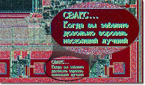
Image courtesy of FSU’s Silicon Zoo
DEC supposedly inscribed the phrase “VAX – When you care enough to steal the very best” on an otherwise-unused area of the die for one of their MicroVAX CPUs. The phrase in the picture reads “СВАКС… Когда вы забатите довольно воровать настоящий лучший” which is horribly mangled Russian, but I think it got the point across.
The highest-performing PDP-11 CPU DEC built was based on the DCJ11 (or J-11, or Jaws), microprocessor. This CPU was the basis for all subsequent DEC PDP-11 products (PDP-11/53, /73, /83, /84, /93 and /94) up until they sold the product line to Mentec, who continued to use the J-11 on their M70 / M71 / M80 / M90 and M100 CPUs. It was not until nearly 4 years had elapsed after Mentec acquired the DEC PDP-11 line that they introduced a new design, the M11, not based on the J-11. This was probably due to the last J-11 chips being manufactured in early 1998, as production was apparently stopped as soon as Compaq acquired DEC.
The J-11 design was not without its problems. It was a joint manufacturing effort of DEC and Harris Semiconductor (Intersil). DEC had previously used the Harris / Intersil 61×0 chips, which implemented the PDP-8 CPU in a microprocessor. They probably weren’t expecting the issues which plagued the J-11 project. In addition to problems with the CPU itself, there were problems with the optional floating-point accelerator chip (designed and built entirely by DEC) and the support chips needed to make the J-11 function in a system. This led to a number of costly recalls by DEC to fix (or conceal) problems. The original distinction between the various PDP-11 systems based on the J-11 was lost as parts (normally the floating-point accelerator chip) were removed and / or the board swapped for a slower 15MHz one in the field to get the systems working reliably. Eventually the J-11 systems became reliable enough that users could have an 18MHz CPU with working floating point. Earlier J-11 chips had speed restrictions (often 15MHz) and did not work with the floating-point chip. The planned optional Commercial Instruction Set (CIS) option was never produced, although you can see where it would have been placed on the bottom side of the CPU.
Certainly not all of the problems were on the Harris side – I’ve successfully run a J-11 at 24MHz on a 3rd-party board. The DEC support chip set was found to be limited to a bit over 18 MHz, which is why DEC did not press Harris particularly hard to meet the 20MHz design goal (for top-binned parts). The part number DCJ11-AE (the -AE suffix indicated the revision level) was the last version produced, the “good one”. Interestingly, the individual chips on the first DCJ11-AE CPUs were revision 1 on the DC334 chip and revision 11 on the DC335. The newest DCJ11-AE I’ve seen (with a module date code of 9820 and chip date codes of 9819) has a revision 4 DC334 chip and a revision 16 DC335 chip. That DCJ11-AE has the Harris logo stamped on the ceramic carrier as well as the individual chips, while a somewhat earlier sample with a 9711 date code has the same revision 4 and 16 chips, but without Harris markings on the ceramic carrier. 9820 is pretty close to the time DEC was acquired by Compaq, so the J-11 hung on to the bitter end, 4 years after DEC sold the rest of the PDP-11 business to Mentec. Apparently there weren’t user-visible changes which would cause the overall CPU revision to change to a DCJ11-AF. Perhaps the changes were to simplify the manufacturing process.
DEC also “shot themselves in the foot” by having one group think the part was solely for DEC’s use in building systems, while another group was trying to get design wins in 3rd-party products. This led to a bizarre situation where if you tried to purchase a J-11 chip by itself from DEC, you got a call from the J-11 product manager (Cathy Berida) who was forced by upper management to ask you what you planned on doing with it before the order would go through. Needless to say, DEC did not get a lot of OEM design wins due to their inconsistent policies regarding the chip. The result of this is that you can purchase case lots of never-used J-11 chips on places like eBay [local copy] if you happen to need a few hundred of them.
[This and all subsequent images in this post are clickable to show a higher-resolution version.]
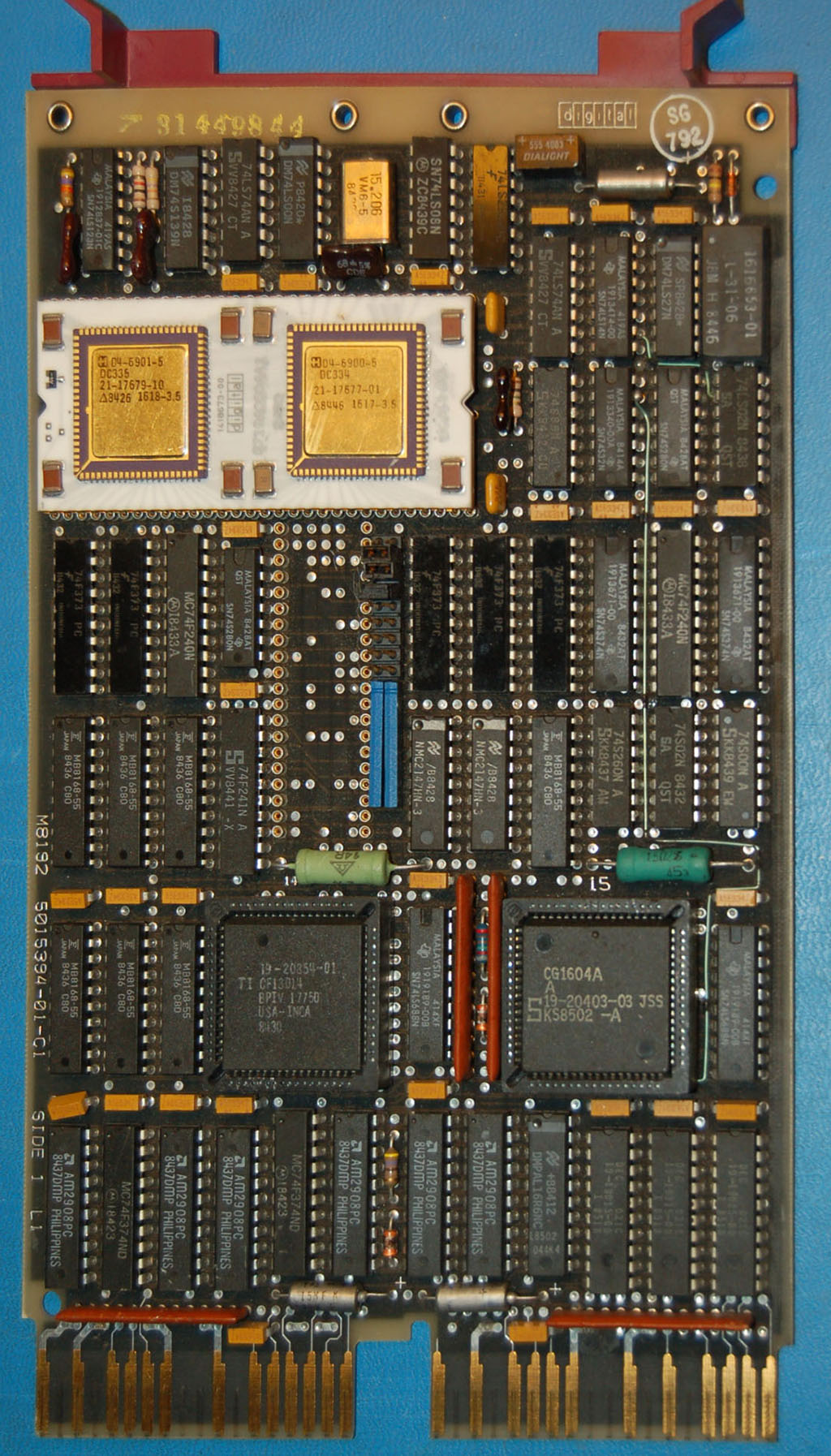
This is a DEC M8192 module, used in the PDP-11/73 systems. It has an older J-11 CPU and no floating-point accelerator (FPA) chip (the large empty socket below the white J-11 CPU). A manual for it is available from Bitsavers [local copy]. Note that the manual doesn’t show the socket for the FPA, and the sole mention of the FPA is in the description of the internal J-11 CPU registers.
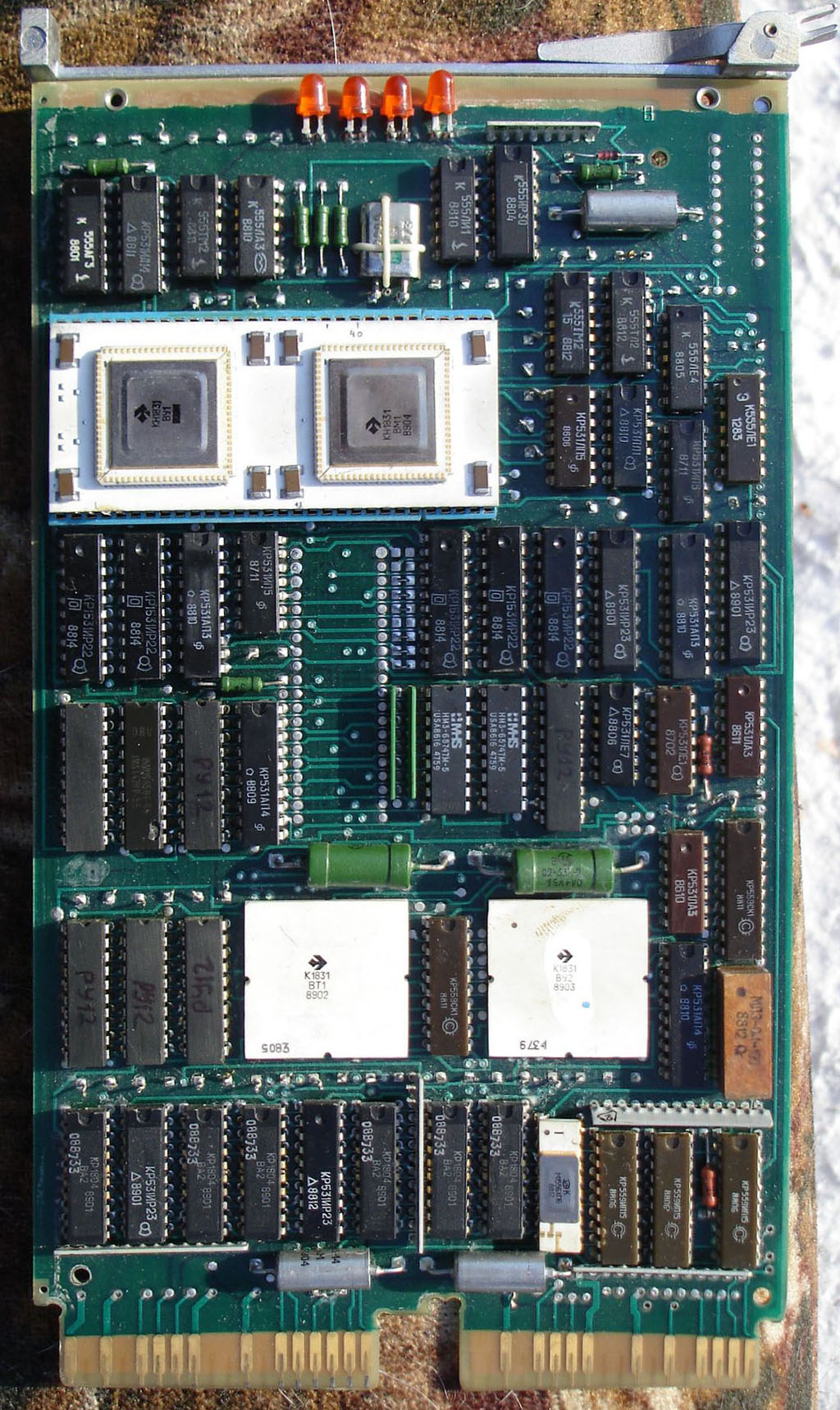
This is a Soviet M8 CPU board. It looks suspiciously like the DEC M8192 board, doesn’t it? Aside from some component substitutions due to limited availability of things (like PLCC sockets for the support chips and the compact 4-LED display) it is pretty much the same board. Note that this board doesn’t even have a socket for the floating-point accelerator chip. The pads are on the board, but there is no socket. This may indicate that the clone parts were created before DEC got the various design issues ironed out. Additionally, the configuration jumpers are soldered in instead of being removable jumpers as they are on the DEC board. The board in the picture is non-functional as some components (mainly bypass capacitors) have been removed for some reason.
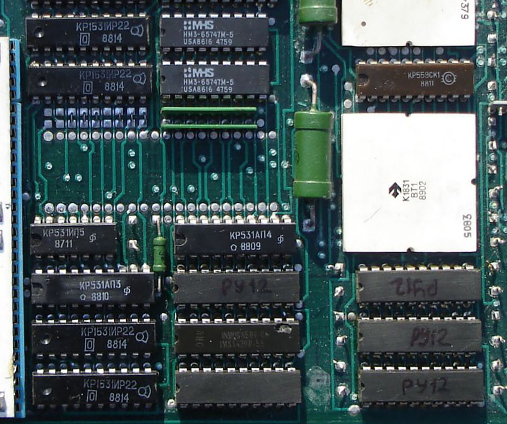
Examining the M8 board in more detail, we can see some very interesting things. At the top center of theis image, you can see two chips with the logo “MHS” and the date code “USA8616”. If you’ve never heard of MHS, I’m not surprised. They were a relatively obscure manufacturer of specialty ICs. MHS stands for “Matra Harris Semiconductor” – yup, the same Harris Semiconductor that was making J-11 parts for DEC. They probably had no idea their parts were ending up in the Soviet Union – often, “front” companies would purchase parts in the West and those parts would eventually make their way into the Soviet Union.
The MHS part is a HM3-65747-5 CMOS 4K x 1 static RAM. The DEC M8192 board, oddly enough, does not use the MHS part. Instead, it uses a National Semiconductor NMC2147HN-3 which appears to be a pin-compatible substitute.
Also in this detail image, you can see 5 parts where the manufacturer and part number information has been ground off and “РУ12” written on on them with a marker pen. There is another of these parts outside the area of this detail. On the DEC M8192, these are Fairchild MB8168-55 NMOS 4K x 4 static RAM. “РУ” was the Soviet type designator for a memory chip. One of the chips on the Soviet board does not have its identifying marks removed, and it appears to be an INMOS IMS1420D-55, also an NMOS 4K x 4 static RAM. The mysterious РУ12 is probably К132РУ12 as this page and this page both show that as an interchange part for the IMS1420-55. They’re almost certainly not Soviet-made parts as there would be no need to grind off the original markings in that case.
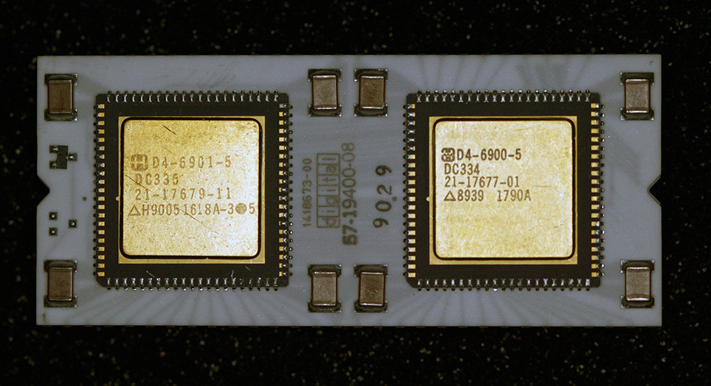
This is the top of a genuine DEC DCJ11-AE. As you can see, there are two large chips mounted to a ceramic carrier. Under the top layer of ceramic you can see some of the leads that connect the two chips to each other and to the pins on the edge of the CPU. There are 4 bypass capacitors for each chip to filter out noise. There is also one SOT-package part (possibly a transistor or 3-terminal regulator) installed, with an unpopulated space for an second one. It possible that the unpopulated space was for a part intended to be used on the underside of the CPU.
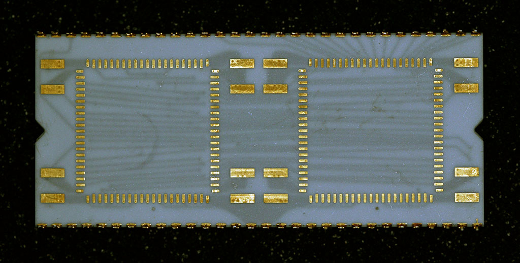
The bottom view of the same part shows the pads which would have held the Commercial Instruction Set if it was ever implemented. You can also see additional leads in an intermediate ceramic layer – the ceramic carrier was a complex, multi-layer affair.
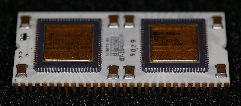
This angle view shows how the individual chips were soldered to the ceramic carrier.
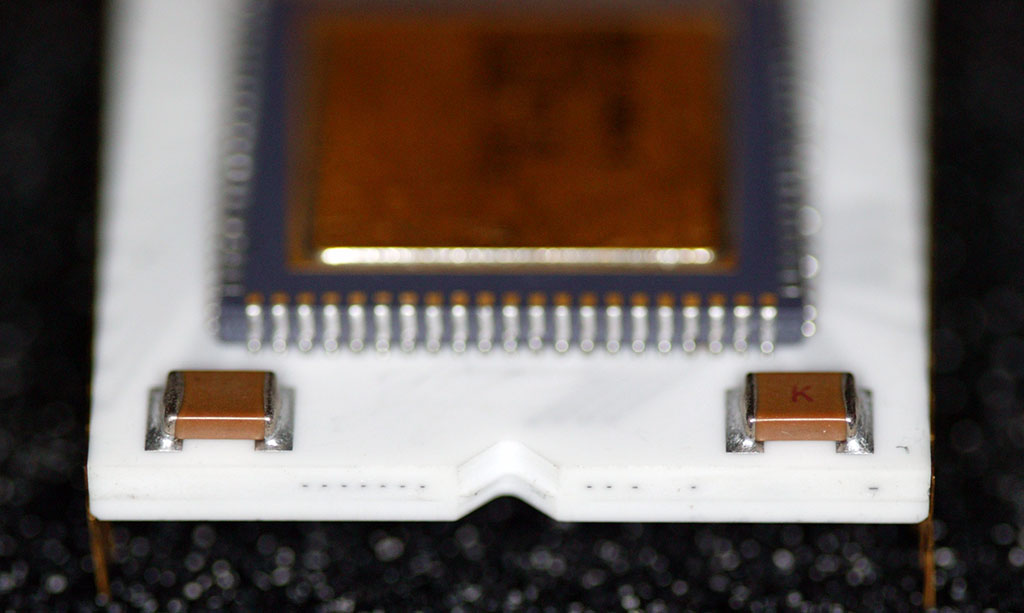
Looking at the edge of the CPU, you can get an idea how thick the ceramic actually is on this part.
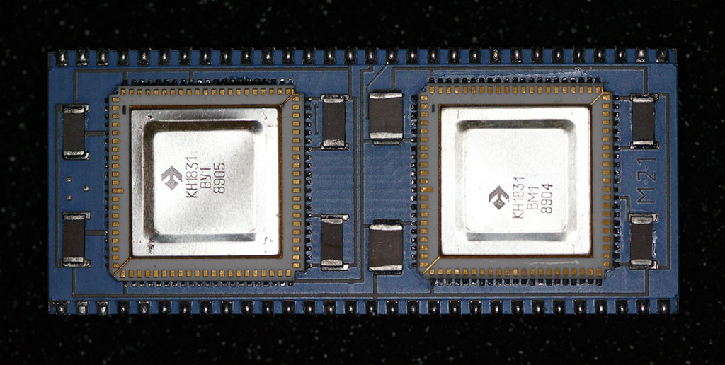
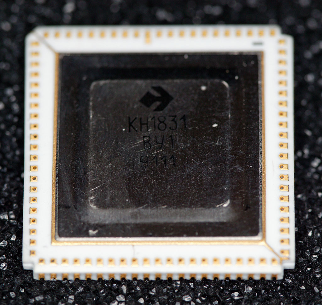
Here is where things get interesting. This is a Soviet 1831 clone of the J-11. The logo on the chips indicates that it was made by the NPO Electronics (НПО Электроника) factory (now VZZP) in Voronezh. Instead of the DC334 and DC335 numbering on the DEC chips, the chips on this board are labeled КН1831ВМ1 and КН1831ВУ1. Wikipedia has a detailed article on Soviet integrated circuit numbering, but it breaks down as follows:
- К – Commercial / consumer component
- Н – Ceramic leadless chip carrier (the individual chips on the CPU carrier)
- 1 – Monolithic integrated circuit
- 8 – Microprocessor
- 31 – Number in series
- ВМ – Microprocessor
- ВУ – Microcode
- 1 – Variant
Apparently the two chips had their own code names – Тунгус 1 (Tungus 1) for the КН1831ВУ1 and Теорема 2 (Theorem 2) for the КН1831ВМ1.
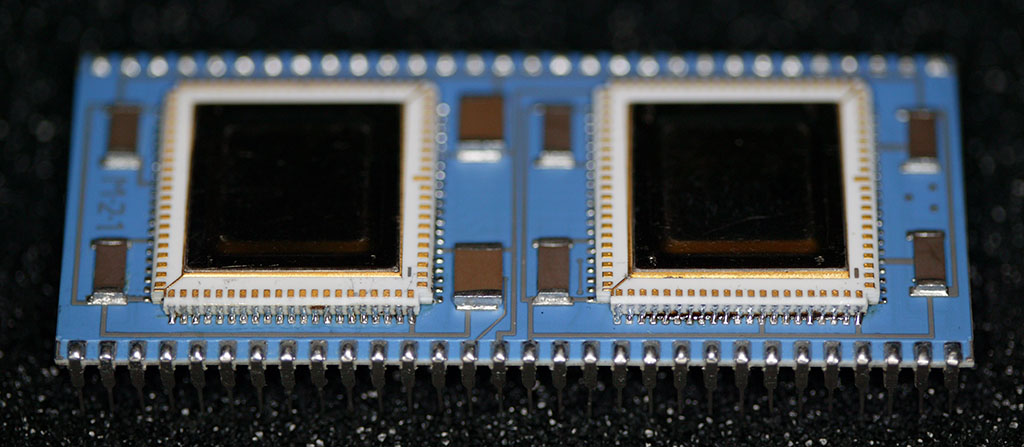
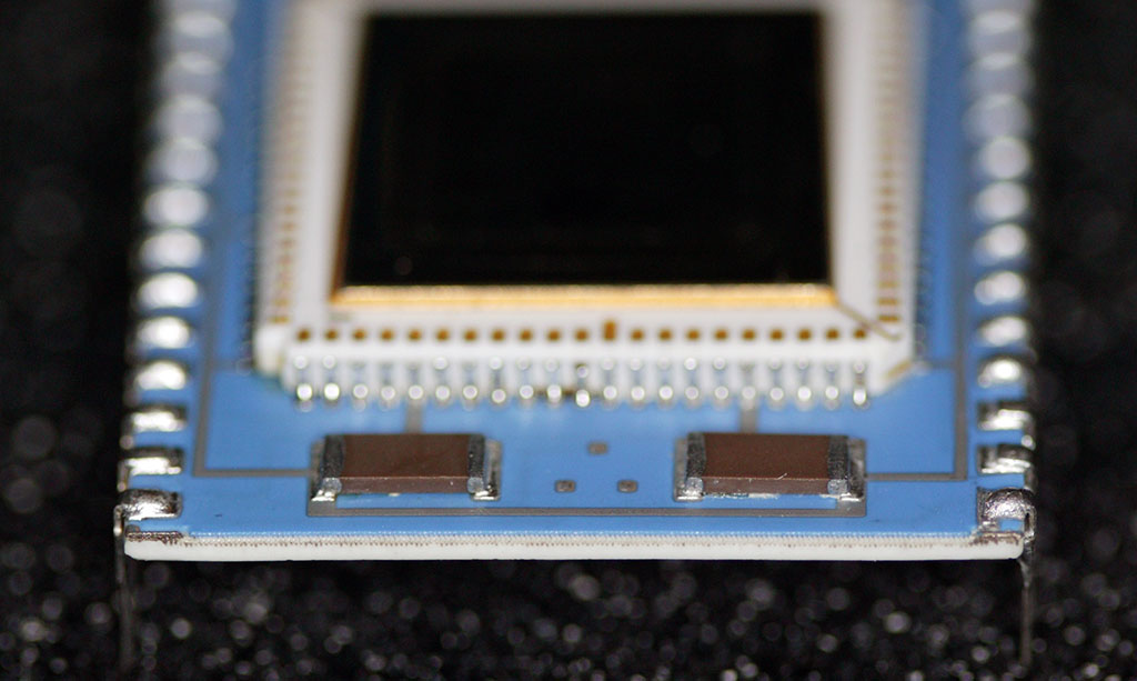
You can see the somewhat different method of attaching the pins to the carrier, compared to the DEC CPU. This is due to the thinner carrier as I will discuss below. The same four bypass capacitors are present, but the SOT-package part found on the J-11 is not, although the pads are there. The chips appear to have been hand-soldered onto the carrier. While the carrier in this picture is blue, variants with white and greenish carriers have been photographed. While this part is just labeled M-2-1, other newer samples have been labeled М8К ред4 (M8K red4).
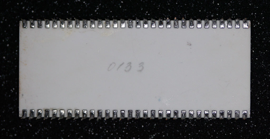
The bottom of the 1831 shows a much simpler method of construction, compared with the DEC J-11. No additional leads are visible and the only marking is “0133”. It is not known what this means – as the chips on the carrier have 8905 and 8904 date codes, it doesn’t make sense that the CPU would have remained unassembled for twelve years. Perhaps it was the date it was installed into or removed from a system?
This angle view clearly shows the hand-soldering of the chips to the carrier.
The edge view shows how much thinner the carrier is compared to the DEC J-11.
This detail shows the top of an unmounted КН1831ВУ1 chip. It is interesting that while the fabrication method was quite different from the DEC version, they apparently went through a lot of effort to match the packaging exactly. Perhaps they were trying to substitute the КН1831ВУ1 and КН1831ВМ1 chips one at a time onto a DEC package during development? That would not explain why this unusual packaging continued into production, though.
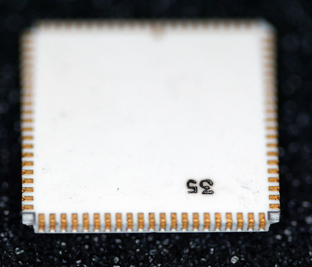
The bottom of the unmounted КН1831ВУ1 is pretty boring, having only a stamped “35”. This does not match the date code on the top of the chip, 9111, so perhaps it is an inspection mark.
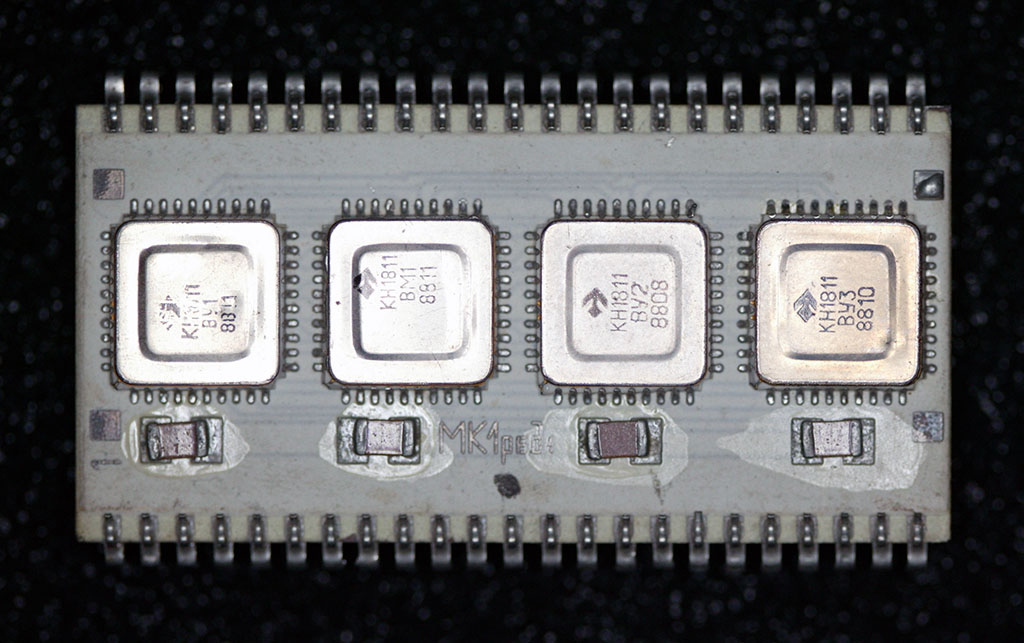
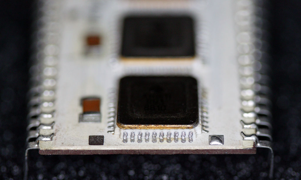
This is an 1811 (DEC F-11, PDP-11/23 and /24) clone CPU. Unlike the 1831, this assembly is not a drop-in equivalent to any DEC F-11. It contains КН1811ВМ1, КН1811ВУ1, КН1811ВУ2 and КН1811ВУ3 chips. That would be a processor and 3 microcode ROMs. This is equivalent to a DEC F-11 and a DEC KEF11-AA FPU (Floating Point Unit). Oddly, in the DEC implementation the KTF11-AA MMU (Memory Management Unit) is necessary for using the KEF11-AA as the FPU reuses some of the registers in the MMU. This chip is marked МК1 ред1 (MK1 red1). The logos on the chips show that they were fabricated by NPO Electronics, same as the J-11 clone.
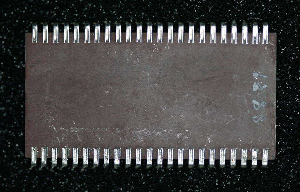
The bottom shows that the CPU is made with a brown ceramic instead of the white ceramic (with blue top coating) used on the 1831. The bottom is marked 8821, which corresponds roughly to the date codes on the individual chips (8808 through 8811). Too faint to be seen clearly is the writing “26-027” across the top of the chip as shown in this picture).
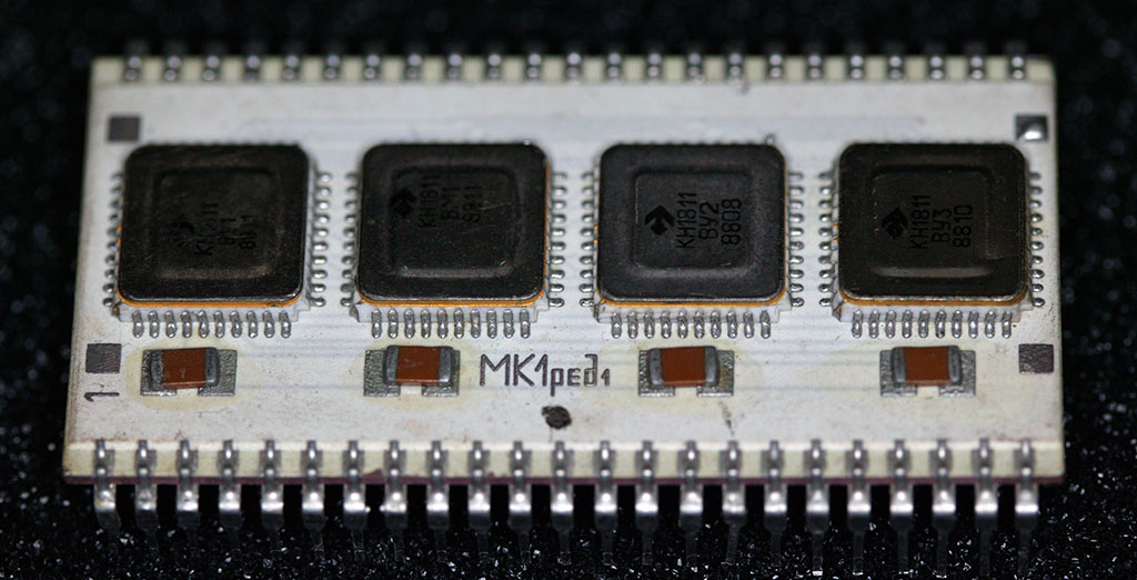
An angle view, clearly showing the “MK1 red1” marking.
Here you can see that the carrier is also quite thin, similar to the 1831.
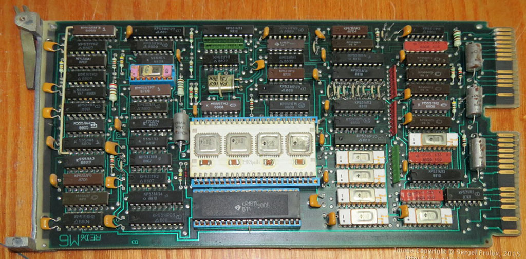
This is the CPU board from the Elektronika 89 minicomputer. You can see the 1811 CPU, along with the КР1811ВТ1 MMU chip, in the center of the board.
I hope you’ve enjoyed this look at a relatively unexplored (in the West) area of computer history. These parts occasionally show up on eBay where they often sell for inflated prices. Not all of the eBay listings have the parts described correctly, so rely on pictures (as long as they’re not “sample image only”) to see what you’re getting.
